- 您現(xiàn)在的位置:買賣IC網(wǎng) > PDF目錄383724 > ORT4622 Field-Programmable System Chip (FPSC) Four-Channel x 622 Mbits/s Backplane Transceiver PDF資料下載
參數(shù)資料
| 型號: | ORT4622 |
| 英文描述: | Field-Programmable System Chip (FPSC) Four-Channel x 622 Mbits/s Backplane Transceiver |
| 中文描述: | 現(xiàn)場可編程系統(tǒng)芯片(促進(jìn)文化基金)四通道x 622 Mbits /秒背板收發(fā)器 |
| 文件頁數(shù): | 45/90頁 |
| 文件大小: | 1915K |
| 代理商: | ORT4622 |
第1頁第2頁第3頁第4頁第5頁第6頁第7頁第8頁第9頁第10頁第11頁第12頁第13頁第14頁第15頁第16頁第17頁第18頁第19頁第20頁第21頁第22頁第23頁第24頁第25頁第26頁第27頁第28頁第29頁第30頁第31頁第32頁第33頁第34頁第35頁第36頁第37頁第38頁第39頁第40頁第41頁第42頁第43頁第44頁當(dāng)前第45頁第46頁第47頁第48頁第49頁第50頁第51頁第52頁第53頁第54頁第55頁第56頁第57頁第58頁第59頁第60頁第61頁第62頁第63頁第64頁第65頁第66頁第67頁第68頁第69頁第70頁第71頁第72頁第73頁第74頁第75頁第76頁第77頁第78頁第79頁第80頁第81頁第82頁第83頁第84頁第85頁第86頁第87頁第88頁第89頁第90頁
Lucent Technologies Inc.
Lucent Technologies Inc.
45
Preliminary Data Sheet
March 2000
ORCA ORT4622 FPSC
Four-Channel x 622 Mbits/s Backplane Transceiver
Timing Characteristics
Description
The most accurate timing characteristics are reported
by the timing analyzer in the ORCAFoundry develop-
ment system. A timing report provided by the develop-
ment system after layout divides path delays into logic
and routing delays. The timing analyzer can also pro-
vide logic delays prior to layout. While this allows rout-
ing budget estimates, there is wide variance in routing
delays associated with different layouts.
The logic timing parameters noted in the Electrical
Characteristics section of this data sheet are the same
as those in the design tools. In the PFU timing, symbol
names are generally a concatenation of the PFU oper-
ating mode and the parameter type. The setup, hold,
and propagation delay parameters, defined below, are
designated in the symbol name by the SET, HLD, and
DEL characters, respectively.
The values given for the parameters are the same as
those used during production testing and speed bin-
ning of the devices. The junction temperature and sup-
ply voltage used to characterize the devices are listed
in the delay tables. Actual delays at nominal tempera-
ture and voltage for best-case processes can be much
better than the values given.
It should be noted that the junction temperature used in
the tables is generally 85 °C. The junction temperature
for the FPGA depends on the power dissipated by the
device, the package thermal characteristics (
Θ
JA
), and
the ambient temperature, as calculated in the following
equation and as discussed further in the Package
Thermal Characteristics Summary section:
T
Jmax =
T
Amax
+ (P
Θ
JA
) °C
Note
: The user must determine this junction tempera-
ture to see if the delays from ORCA Foundry
should be derated based on the following derat-
ing tables.
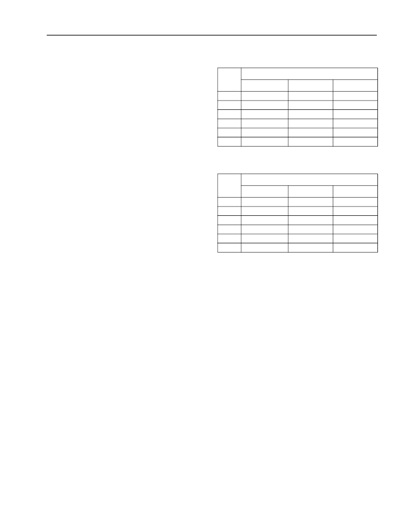
Table 27 and Table 28 provide approximate power sup-
ply and junction temperature derating for OR3LP26B
commercial devices. The delay values in this data
sheet and reported by ORCA Foundry are shown as
1.00 in the tables. The method for determining the
maximum junction temperature is defined in the Pack-
age Thermal Characteristics section. Taken cumula-
tively, the range of parameter values for best-case vs.
worst-case processing, supply voltage, and junction
temperature can approach three to one.
Table 27. Derating for Commercial Devices (I/O
Supply V
DD
)
Table 28. Derating for Commercial Devices (I/O
Supply V
DD
2)
Note: The derating tables shown above are for a typical critical path
that contains 33% logic delay and 66% routing delay. Since the
routing delay derates at a higher rate than the logic delay,
paths with more than 66% routing delay will derate at a higher
rate than shown in the table. The approximate derating values
vs. temperature are 0.26% per °C for logic delay and 0.45%
per °C for routing delay. The approximate derating values vs.
voltage are 0.13% per mV for both logic and routing delays at
25 °C.
T
J
(°C)
Power Supply Voltage
3.0 V
0.82
0.91
0.98
1.00
1.23
1.34
3.3 V
0.72
0.80
0.85
0.99
1.07
1.15
3.6 V
0.66
0.72
0.77
0.90
0.94
1.01
–40
0
25
85
100
125
T
J
(°C)
Power Supply Voltage
2.38 V
0.86
0.94
0.99
1.00
1.23
1.33
2.5 V
0.71
0.79
0.84
0.99
1.05
1.13
2.63 V
0.67
0.73
0.77
0.92
0.96
1.03
–40
0
25
85
100
125
相關(guān)PDF資料 |
PDF描述 |
|---|---|
| ort551 | Reed Switch(舌簧開關(guān)) |
| ord2210v | Reed Switch(舌簧開關(guān)) |
| ord2210 | Reed Switch(舌簧開關(guān)) |
| ord211 | Reed Switch(舌簧開關(guān)) |
| ord2211 | Reed Switch(舌簧開關(guān)) |
相關(guān)代理商/技術(shù)參數(shù) |
參數(shù)描述 |
|---|---|
| ORT4622BC432-DB | 功能描述:FPGA - 現(xiàn)場可編程門陣列 10368 LUT 204 I/O RoHS:否 制造商:Altera Corporation 系列:Cyclone V E 柵極數(shù)量: 邏輯塊數(shù)量:943 內(nèi)嵌式塊RAM - EBR:1956 kbit 輸入/輸出端數(shù)量:128 最大工作頻率:800 MHz 工作電源電壓:1.1 V 最大工作溫度:+ 70 C 安裝風(fēng)格:SMD/SMT 封裝 / 箱體:FBGA-256 |
| ORT551 | 制造商:Hasco Components International Corp 功能描述: |
| ORT551(1315) | 制造商:OKI Semiconductor 功能描述: |
| ORT551/10-15 AT | 功能描述:磁性/簧片開關(guān) 1 Form C 14mm AT 1015 OKI RoHS:否 制造商:MEDER electronic (Standex) 開關(guān)類型:Reed 觸點(diǎn)形式:1 Form A (SPST-NO) 觸點(diǎn)額定值:10 VA 操作范圍:10 At to 50 At 工作間隙: 磁鐵類型: 顏色: 端接類型:Axial 封裝:Bulk |
| ORT551-1/10-15 AT | 功能描述:磁性/簧片開關(guān) 1 Form C 14mm AT1015 Formed Ld OKI RoHS:否 制造商:MEDER electronic (Standex) 開關(guān)類型:Reed 觸點(diǎn)形式:1 Form A (SPST-NO) 觸點(diǎn)額定值:10 VA 操作范圍:10 At to 50 At 工作間隙: 磁鐵類型: 顏色: 端接類型:Axial 封裝:Bulk |
發(fā)布緊急采購,3分鐘左右您將得到回復(fù)。