- 您現(xiàn)在的位置:買賣IC網(wǎng) > PDF目錄368122 > PS20351-G (POWEREX INC) Intellimod⑩ Module Dual-In-Line Intelligent Power Module 3 Amperes/500 Volts PDF資料下載
參數(shù)資料
| 型號(hào): | PS20351-G |
| 廠商: | POWEREX INC |
| 元件分類: | 運(yùn)動(dòng)控制電子 |
| 英文描述: | Intellimod⑩ Module Dual-In-Line Intelligent Power Module 3 Amperes/500 Volts |
| 中文描述: | AC MOTOR CONTROLLER, 6 A, UFM26 |
| 封裝: | POWER, MINI, DIP-26 |
| 文件頁數(shù): | 9/9頁 |
| 文件大小: | 183K |
| 代理商: | PS20351-G |
MITSUBISHI SEMICONDUCTOR <Intelligent Power Module>
PS20351-N
TRANSFER-MOLD TYPE
INSULATED TYPE
Sep. 2001
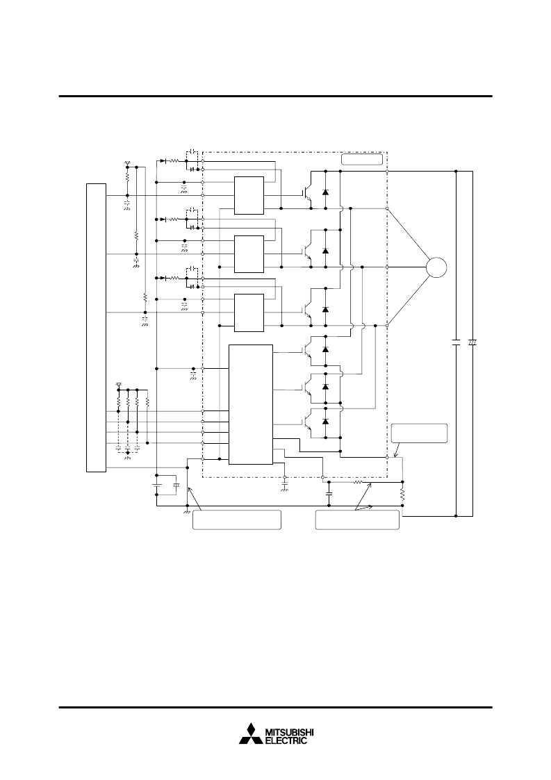
Fig. 7 TYPICAL DIP-IPM APPLICATION CIRCUIT EXAMPLE
Note 1:
To prevent the input signals oscillation, an RC coupling at each input is recommended, and the wiring of each input should be as short
as possible (less than 2cm).
2:
By virtue of integrating an application specific type HVIC inside the module, direct coupling to CPU terminals without any opto-coupler
or transformer isolation is possible.
3:
F
O
output is open collector type. This signal line should be pulled up to the positive side of the 5V power supply with approximately
5.1k
resistance.
4:
F
O
output pulse width should be decided by connecting an external capacitor between CFO and V
NC
terminals (C
FO
). (Example : C
FO
= 22 nF
→
t
FO
= 1.8 ms (typ.))
5:
Each input signal line should be pulled up to the positive side of the 5V power supply with approximately 4.7k
resistance (other RC
coupling circuits at each input may be needed depending on the PWM control scheme used and on the wiring impedances of the
system
’
s printed circuit board). Approximately a 0.22~2
μ
F by-pass capacitor should be used across each power supply connection
terminals.
6:
To prevent errors of the protection function, the wiring of A, B, C should be as short as possible.
7:
In the recommended protection circuit, please select the R
1
C
5
time constant in the range of 1.5~2
μ
s.
8:
Each capacitor should be put as nearby the terminals of the DIP-IPM as possible.
9:
To prevent surge destruction, the wiring between the smoothing capacitor and the P&N1 terminals should be as short as possible. Ap-
proximately a 0.1~0.22
μ
F snubber capacitor between the P&N1 terminals is recommended.
HO
HO
DIP-IPM
C3
C3
C3
C3
C2
C2
C2
C1
C1
C1
HO
IN
IN
IN
COM
COM
COM
U
OUT
V
OUT
W
OUT
V
NO
CFO
GND
F
o
W
N
V
N
V
CC
C
B
A
C4(C
FO
)
CFO
R1
C5
CIN
CIN
N1
N
W
V
U
P
V
S
V
S
V
S
V
B
V
B
V
B
V
CC
V
CC
V
CC
Fo
W
N
V
N
U
N
U
N
W
P
V
P
U
P
V
NC
V
N1
V
P1
V
P1
V
P1
HVIC1
HVIC2
HVIC3
LVIC
V
WFS
V
VFS
V
UFS
V
WFB
V
VFB
V
UFB
M
Shunt
resistor
The long wiring of GND might generate
noise on input signals and cause IGBT
to be malfunctioned.
If this wiring is too long, the SC level
fluctuation might be large and cause
SC malfunction.
If this wiring is too long,
short circuit might
be caused.
15V line
5V line
U
N
I
T
C
P
U
5V line
C1: Tight tolerance temp-compensated electrolytic type; C2,C3: 0.22~2
μ
F R-category ceramic capacitor for noise filtering
相關(guān)PDF資料 |
PDF描述 |
|---|---|
| PS2045(中文) | Precision Voltage Supervisor(帶看門狗定時(shí)器和4K IIC存儲(chǔ)器的精密電壓監(jiān)控電路(適用于3和5伏系統(tǒng))) |
| PS2101(中文) | Serial Output Data Acquisition Circuit(串行輸出數(shù)據(jù)采集芯片) |
| PS2103(中文) | Serial Output Data Acquisition Circuit(串行輸出數(shù)據(jù)采集芯片) |
| PS21204 | TRANSFER-MOLD TYPE INSULATED TYPE |
| PS21205 | TRANSFER-MOLD TYPE INSULATED TYPE |
相關(guān)代理商/技術(shù)參數(shù) |
參數(shù)描述 |
|---|---|
| PS20351-GP | 制造商:MITSUBISHI 制造商全稱:Mitsubishi Electric Semiconductor 功能描述:Generation DIP and Mini-DIP-IPM |
| PS20351-N | 制造商:MITSUBISHI 制造商全稱:Mitsubishi Electric Semiconductor 功能描述:TRANSFER-MOLD TYPE INSULATED TYPE |
| PS20351-NP | 制造商:MITSUBISHI 制造商全稱:Mitsubishi Electric Semiconductor 功能描述:Generation DIP and Mini-DIP-IPM |
| PS204 | 制造商:PANJIT 制造商全稱:Pan Jit International Inc. 功能描述:PLASTIC SILICON RECTIFIER |
| PS2041 | 制造商:NEC 制造商全稱:NEC 功能描述:HIGH SPEED 6 PIN PHOTO COUPLER |
發(fā)布緊急采購(gòu),3分鐘左右您將得到回復(fù)。