- 您現(xiàn)在的位置:買賣IC網(wǎng) > PDF目錄230919 > RDC-19222-202 (DATA DEVICE CORP) SYNCHRO OR RESOLVER TO DIGITAL CONVERTER, PQCC44 PDF資料下載
參數(shù)資料
| 型號: | RDC-19222-202 |
| 廠商: | DATA DEVICE CORP |
| 元件分類: | 位置變換器 |
| 英文描述: | SYNCHRO OR RESOLVER TO DIGITAL CONVERTER, PQCC44 |
| 封裝: | PLASTIC, LCC-44 |
| 文件頁數(shù): | 21/24頁 |
| 文件大?。?/td> | 1233K |
| 代理商: | RDC-19222-202 |
6
Data Device Corporation
www.ddc-web.com
RDC-19220 SERIES
V-12/08-0
4) The BIT output which is active low is activated by an error of
approximately 100 LSBs. During normal operation for step
inputs or on power up, a large error can exist.
5) This device has several high impedance amplifier inputs (+C,
-C, +S, -S, -VCO and -VSuM). These nodes are sensitive to
noise and coupling components should be connected as
close as possible.
6) Setup of bandwidth and velocity scaling for the optimized
critically damped case example as follows [Note: DDC has
external component selection software that considers all the
criteria below and, in a simple fashion, asks the key parame-
ters (carrier frequency, resolution, bandwidth, and tracking
rate) to derive the external component values].
- Select the desired f BW (closed loop) based on overall
system dynamics.
- Select f carrier > 3.5f BW
- Select the applications tracking rate (in accordance with TABLE 3),
and use appropriate values for R SET and R CLK
- Compute Rv =
- Compute CBW (pF) =
- Where Fs = 67 kHz for R CLK = 30 K
100 kHz for R CLK = 20 K
125 kHz for R CLK = 15 K
- Compute RB =
- Compute
3.2 x Fs (Hz) x 108
Rv x (f BW)2
Full Scale Velocity Voltage
Tracking Rate (rps) x 2 resolution x 50 pF x 1.25 V
0.9
CBW x f BW
CBW
10
As an example:
Calculate component values for a 16-bit converter with 100Hz
bandwidth, a tracking rate of 10RPS and a full scale velocity
of 4 volts.
- Rv =
= 97655
- Compute CBW (pF) =
= 21955 pF
- Compute RB =
= 410 k
4 V
10 rps x 216 x 50 pF x 1.25 V
0.9
21955 x 10 -12 x 100 Hz
3.2 x 67 kHz x 108
97655 x 100 Hz2
Note: DDC has software available to perform the previous calcu-
lations. Contact DDC to request software or visit our web-
site at www.ddc-web.com to download software.
7) Selecting a fbw that is too low relative to the maximum appli-
cation tracking rate can create a spin-around condition in
which the converter never settles. The relationship to insure
against
spin-around
is
as
follows
(TABLE
3):
8)
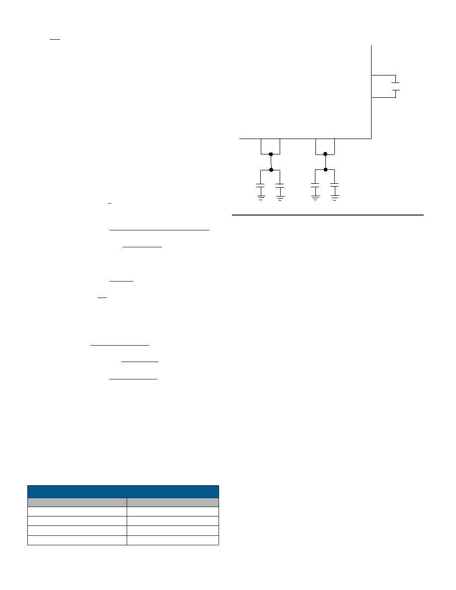
For Rdc-19222 & Rdc-19224 packages only.
This version is capable of +5V only operation. It accomplishes
this with a charge pump technique that inverts the +5V supply
for use as -5V, hence the +5V supply current doubles. The
built-in -5 V inverter can be used by connecting pin 2 to 26,
pin 17 to 22, a 10 F/10 Vdc capacitor from pin 23 (negative
terminal) to pin 25 (positive terminal), and a 47 F/10 Vdc
capacitor from -5 V to gND. The current drain from the +5 V
supply doubles. No external -5 V supply is needed (SEE
FIguRE 5).
When using the -5 V inverter, the max. tracking rate should be
scaled for a velocity output of 3.5 V max. use the following equa-
tion to determine tracking rate used in the formula on page 5:
TR (required) x (4.0) = Tracking rate used in calculation
(3.5)
Note: When using the highest BW and Tracking Rates, using
the -5 V inverter is not recommended.
HIgHER TRACKINg RATES AND CARRIER FREQuENCIES
Tracking rate (nominally 4 V) is limited by two factors: velocity
voltage saturation and maximum internal clock rate (nominally
1,333,333 Hz). An understanding of their interaction is essential
to extending performance.
The general Setup Considerations section makes note of the
selection of Rv for the desired velocity scaling. Rv is the input
resistor to an inverting integrator with a 50 pF nominal feedback
capacitor. When it integrates to -1.25 V, the converter counts up 1
LSB and when it integrates to +1.25 V, the converter counts down
1 LSB. When a count is taken, a charge is dumped on the capac-
ity.
RDC-19222/4
10uF
+CAP
-CAP
.01uF
(-5c) -5V
.01uF
(+5c) +5V
47uF
+
FIGURE 5. -5V BUILT-IN INVERTER
TABLE 3. TRAcKING/BW RELATIONsHIP
RPs (MAx)/BW
REsOLUTION
1
10
0.45
12
0.25
14
0.125
16
相關(guān)PDF資料 |
PDF描述 |
|---|---|
| RD-14591F1-232Q | SYNCHRO OR RESOLVER TO DIGITAL CONVERTER, CDMA36 |
| RDC-630-A-L-1-R | SYNCHRO OR RESOLVER TO DIGITAL CONVERTER, DMA27 |
| RD-14595F5-414 | SYNCHRO OR RESOLVER TO DIGITAL CONVERTER, CDFP36 |
| RD-14590F1-524L | SYNCHRO OR RESOLVER TO DIGITAL CONVERTER, CDMA36 |
| RD-14590F1-804L | SYNCHRO OR RESOLVER TO DIGITAL CONVERTER, CDMA36 |
相關(guān)代理商/技術(shù)參數(shù) |
參數(shù)描述 |
|---|---|
| RDC-19222-202T | 制造商:未知廠家 制造商全稱:未知廠家 功能描述:LVDT/Resolver-to-Digital Converter |
| RDC-19222-203 | 制造商:未知廠家 制造商全稱:未知廠家 功能描述:LVDT/Resolver-to-Digital Converter |
| RDC-19222-203T | 制造商:未知廠家 制造商全稱:未知廠家 功能描述:LVDT/Resolver-to-Digital Converter |
| RDC-19222-301 | 制造商:未知廠家 制造商全稱:未知廠家 功能描述:LVDT/Resolver-to-Digital Converter |
| RDC19222-301 | 制造商: 功能描述: 制造商:undefined 功能描述: |
發(fā)布緊急采購,3分鐘左右您將得到回復(fù)。