- 您現(xiàn)在的位置:買賣IC網(wǎng) > PDF目錄373273 > RH80532NC029256 Microprocessor PDF資料下載
參數(shù)資料
| 型號(hào): | RH80532NC029256 |
| 元件分類: | 微處理器 |
| 英文描述: | Microprocessor |
| 中文描述: | 微處理器 |
| 文件頁數(shù): | 73/93頁 |
| 文件大小: | 2353K |
| 代理商: | RH80532NC029256 |
第1頁第2頁第3頁第4頁第5頁第6頁第7頁第8頁第9頁第10頁第11頁第12頁第13頁第14頁第15頁第16頁第17頁第18頁第19頁第20頁第21頁第22頁第23頁第24頁第25頁第26頁第27頁第28頁第29頁第30頁第31頁第32頁第33頁第34頁第35頁第36頁第37頁第38頁第39頁第40頁第41頁第42頁第43頁第44頁第45頁第46頁第47頁第48頁第49頁第50頁第51頁第52頁第53頁第54頁第55頁第56頁第57頁第58頁第59頁第60頁第61頁第62頁第63頁第64頁第65頁第66頁第67頁第68頁第69頁第70頁第71頁第72頁當(dāng)前第73頁第74頁第75頁第76頁第77頁第78頁第79頁第80頁第81頁第82頁第83頁第84頁第85頁第86頁第87頁第88頁第89頁第90頁第91頁第92頁第93頁
Mobile Intel
Pentium
4 Processor-M
250686-002
Datasheet
73
C11
VSS
Power/Other
C12
VCC
Power/Other
C13
VSS
Power/Other
C14
VCC
Power/Other
C15
VSS
Power/Other
C16
VCC
Power/Other
C17
VSS
Power/Other
C18
VCC
Power/Other
C19
VSS
Power/Other
C20
VCC
Power/Other
C21
D#[04]
Source Synch
Input/Output
C22
VSS
Power/Other
C23
D#[07]
Source Synch
Input/Output
C24
D#[08]
Source Synch
Input/Output
C25
VSS
Power/Other
C26
D#[12]
Source Synch
Input/Output
D1
LINT0
Asynch GTL+
Input
D2
BPRI#
Common Clock
Input
D3
VSS
Power/Other
D4
TCK
TAP
Input
D5
TDO
TAP
Output
D6
VSS
Power/Other
D7
VCC
Power/Other
D8
VSS
Power/Other
D9
VCC
Power/Other
D10
VSS
Power/Other
D11
VCC
Power/Other
D12
VSS
Power/Other
D13
VCC
Power/Other
D14
VSS
Power/Other
D15
VCC
Power/Other
D16
VSS
Power/Other
D17
VCC
Power/Other
D18
VSS
Power/Other
D19
VCC
Power/Other
D20
VSS
Power/Other
D21
VSS
Power/Other
D22
D#[05]
Source Synch
Input/Output
D23
D#[13]
Source Synch
Input/Output
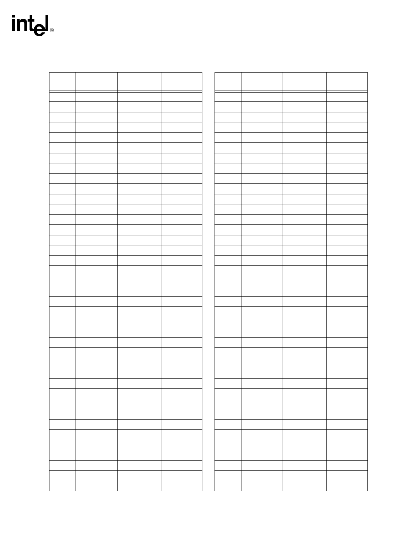
Table 35. Pin Listing by Pin Number
Pin
Number
Pin Name
Signal Buffer
Type
Direction
D24
VSS
Power/Other
D25
D#[15]
Source Synch
Input/Output
D26
D#[23]
Source Synch
Input/Output
E1
VSS
Power/Other
E2
DEFER#
Common Clock
Input
E3
HITM#
Common Clock
Input/Output
E4
VSS
Power/Other
E5
LINT1
Asynch GTL+
Input
E6
TRST#
TAP
Input
E7
VSS
Power/Other
E8
VCC
Power/Other
E9
VSS
Power/Other
E10
VCC
Power/Other
E11
VSS
Power/Other
E12
VCC
Power/Other
E13
VSS
Power/Other
E14
VCC
Power/Other
E15
VSS
Power/Other
E16
VCC
Power/Other
E17
VSS
Power/Other
E18
VCC
Power/Other
E19
VSS
Power/Other
E20
VCC
Power/Other
E21
DBI#[0]
Source Synch
Input/Output
E22
DSTBN#[0]
Source Synch
Input/Output
E23
VSS
Power/Other
E24
D#[17]
Source Synch
Input/Output
E25
D#[21]
Source Synch
Input/Output
E26
VSS
Power/Other
F1
RS#[0]
Common Clock
Input
F2
VSS
Power/Other
F3
HIT#
Common Clock
Input/Output
F4
RS#[2]
Common Clock
Input
F5
VSS
Power/Other
F6
GTLREF
Power/Other
Input
F7
TMS
TAP
Input
F8
VSS
Power/Other
F9
VCC
Power/Other
F10
VSS
Power/Other
Table 35. Pin Listing by Pin Number
Pin
Number
Pin Name
Signal Buffer
Type
Direction
相關(guān)PDF資料 |
PDF描述 |
|---|---|
| RH80532NC033256 | Microprocessor |
| RHE070 | Poly Switch PTC DEVICES |
| RHE1000 | Poly Switch PTC DEVICES |
| RHE1300 | Poly Switch PTC DEVICES |
| RHE1500 | Poly Switch PTC DEVICES |
相關(guān)代理商/技術(shù)參數(shù) |
參數(shù)描述 |
|---|---|
| RH80532NC033256 | 制造商:未知廠家 制造商全稱:未知廠家 功能描述:Microprocessor |
| RH80532NC049256 | 制造商:Rochester Electronics LLC 功能描述:- Bulk |
| RH80532NC049256S L8SB | 制造商:Intel 功能描述:INTEL CELERON PROCESSOR AVAILABLE AT 1.60 GHZ, 1.8 GHZ, 2.00 GHZ, 2.2 GHZ |
| RH80532NC049256S-L8SB | 制造商:Intel 功能描述:INTEL CELERON PROCESSOR AVAILABLE AT 1.60 GHZ, 1.8 GHZ, 2.00 GHZ, 2.2 GHZ |
| RH80532NC056256 | 制造商:Rochester Electronics LLC 功能描述:- Bulk |
發(fā)布緊急采購,3分鐘左右您將得到回復(fù)。