- 您現(xiàn)在的位置:買賣IC網(wǎng) > PDF目錄368518 > RM2207D (Raytheon Company) Voltage Controlled Oscillator PDF資料下載
參數(shù)資料
| 型號: | RM2207D |
| 廠商: | Raytheon Company |
| 英文描述: | Voltage Controlled Oscillator |
| 中文描述: | 壓控振蕩器 |
| 文件頁數(shù): | 4/12頁 |
| 文件大?。?/td> | 74K |
| 代理商: | RM2207D |
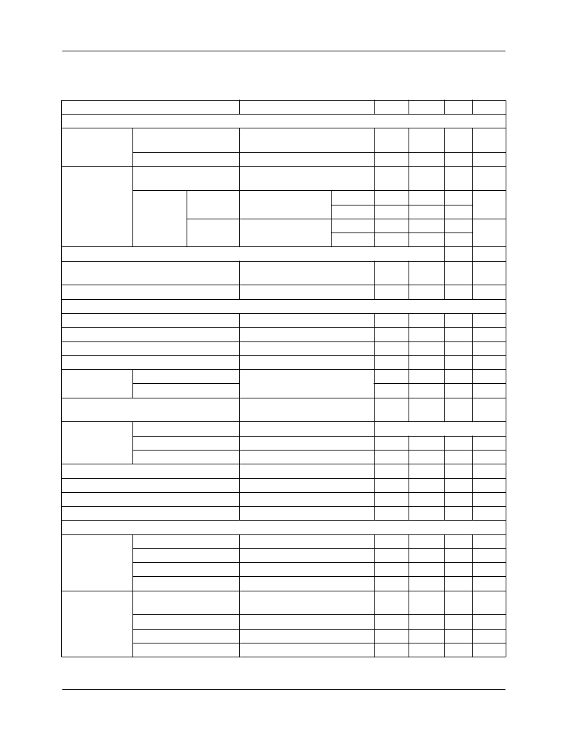
RC2207
PRODUCT SPECIFICATION
4
Electrical Characteristics
(Test Circuit of Figure 1, V
grounded, S1 and S2 closed unless otherwise specified)
S
=
±
6V, T
A
= +25
°
C, C = 5000 pF, R1= R2 = R3 = R4 = 20 k
, R
L
= 4.7
binary inputs
Note:
1. Guaranteed by design.
Parameters
General Characteristics
Supply Voltage
Test Conditions
Min.
Typ.
Max.
Units
Single Supply
See Typical Performance
Characteristics
+8.0
+12
+26
V
Split Supplies
Single Supply
±
4
±
5.0
6
±
7.0
13
V
Supply Current
Measured at pin 1,
S1 open (See Fig. 8)
Measured at pin 1,
S1 open (See Fig. 7)
mA
Split
Supplies
Positive
RC2207
RM2207
RC2207
RM2207
5.0
7.0
8.0
7.0
6.0
mA
Negative
Measured at pin 12,
S1, S2 open
mA
4.0
Binary Keying Inputs
Switching Threshold
Measured at pins 8 and 9.
Refer to pin 10.
1.4
2.2
2.8
V
Input Resistance
Oscillator Section—Frequency Characteristics
Upper Frequency Limit
Lower Practical Frequency
Frequency Accuracy
Frequency Matching
Frequency
Stability
vs. Supply Voltage
Sweep Range
5.0
k
C = 500 pF, R3 = 2 k
C = 50
μ
F, R3 = 2 k
0.5
1.0
0.01
±
1.0
0.5
20
0.15
3000:1
MHz
Hz
% of f
% of f
ppm/
%/V
f
H
±
3.0
0
0
C
vs. Temperature (Note 1)
0
°
C < T
A
< +70
°
C
50
°
R3 = 1.5 k
R3 = 2 M
C = 5000 pF
f
H
= 10 kHz, f
f
H
= 100 kHz, f
±
10% FM Deviation
See Characteristic Curves
Measured at pins 4, 5, 6, or 7
for f
for f
H
L
1000:1
/f
L
Sweep Linearity
10:1 Sweep
1000:1 Sweep
1
L
= 1 kHz
= 100 Hz
1.0
5.0
0.1
2.0
%
%
%
k
mV
L
FM Distortion
Recommended Range of Timing Resistors
Impedance at Timing Pins
DC Level at Timing Terminals
Output Characteristics
Triangle output
Amplitude
Impedance
DC Level
Linearity
Squarewave
Output
Saturation Voltage
Rise Time
Fall Time
1.5
2000
75
10
Measured at pin 14
4
6
V
P-P
mV
%
V
P-P
10
Referenced to pin 10
from 10% to 90% of swing
Measured at pin 13,
S2 Closed
Referenced to pin 12
C
L
≤
10 pF
C
L
≤
10 pF
+100
0.1
12
Amplitude
11
0.2
200
20
0.4
V
ns
ns
相關PDF資料 |
PDF描述 |
|---|---|
| RM2A | SILICON RECTIFIER DIODES |
| RM2Z | SILICON RECTIFIER DIODES |
| RM2B | SILICON RECTIFIER DIODES |
| RM2C | SILICON RECTIFIER DIODES |
| RM4190D | RADIATION HARDENED HIGH EFFICIENCY, 5 AMP SWITCHING REGULATORS |
相關代理商/技術參數(shù) |
參數(shù)描述 |
|---|---|
| RM2207D/883B | 制造商:QP Semiconductor 功能描述:VOLTAGE CONTROLLED OSCILLATOR |
| RM2207D8 | 制造商:Fairchild Semiconductor Corporation 功能描述:QT# DVQR56 |
| RM220C | 制造商:未知廠家 制造商全稱:未知廠家 功能描述:Logic IC |
| RM220D | 制造商:未知廠家 制造商全稱:未知廠家 功能描述:Logic IC |
| RM220M | 制造商:未知廠家 制造商全稱:未知廠家 功能描述:R. F. Molded Chokes |
發(fā)布緊急采購,3分鐘左右您將得到回復。