- 您現(xiàn)在的位置:買賣IC網(wǎng) > PDF目錄368518 > RM2207D (Raytheon Company) Voltage Controlled Oscillator PDF資料下載
參數(shù)資料
| 型號(hào): | RM2207D |
| 廠商: | Raytheon Company |
| 英文描述: | Voltage Controlled Oscillator |
| 中文描述: | 壓控振蕩器 |
| 文件頁(yè)數(shù): | 6/12頁(yè) |
| 文件大小: | 74K |
| 代理商: | RM2207D |
RC2207
PRODUCT SPECIFICATION
6
Applications Information
Precautions
The following precautions should be observed when
operating the RC2207 family of integrated circuits:
Pulling excessive current from the timing terminals will
adversely affect the temperature stability of the circuit. To
minimize this disturbance, it is recommended that the
total current drawn from pins 4, 5, 6 and 7 be limited to <6
mA. In addition, permanent damage to the device may
occur if the total timing current exceeds 10 mA.
Terminals 2, 3, 4, 5, 6 and 7 have very low internal
impedance and should, therefore, be protected from
accidental shorting to ground or the supply voltages.
The keying logic pulse amplitude should not exceed the
supply voltage.
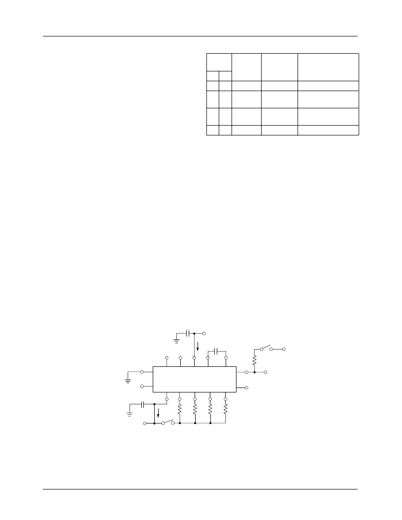
Split Supply Operation
Figure 7 is the recommended circuit connection for split
supply operation. The frequency of operation is determined
by the timing capacitor (C) and the activated timing resistors
(R1 through R4). The timing resistors are activated by the
logic signals at the binary keying inputs (pins 8 and 9), as
shown in Table 1. If a single timing resistor activated, the
frequency is 1/RC.
Otherwise, the frequency is either 1/(R1| |R2)C or
1/(R1| |R4)C.
Table 1. Logic Table for Binary Keying Controls
Note:
1. For single supply operation, logic levels are referenced to
voltage at pin 10.
The squarewave output is obtained at pin 13 and has a
peak-to-peak voltage swing equal to the supply voltages.
This output is an open-collector type and requires an
external pull-up load resistor (nominally 5 k
) to the posi-
tive supply. The triangle waveform obtained at pin 14 is cen-
tered about ground and has a peak amplitude of +V
S
/2.
The circuit operates with supply voltages ranging from
±
4V
to it
±
13V. Minimum drift occurs with
±
6V supplies.
Single Supply Operation
The circuit should be interconnected as shown in Figure 8
for single supply operation. Pin 12 should be grounded, and
pin 11 biased from +V
S
through a resistive divider to a value
of bias voltage between +V
S
/3 and +V
S
/2. Pin 10 is
bypassed to ground through a 0.1
μ
F capacitor.
Logic
Level
8
0
0
Selected
Timing
Pins
f1
6 & 7
Frequency
f
1
= 1/R3C
f
1
+
f
1
Definitions
f1 = 1/R4C
f
2
= 1/R2C,
f
2
= 1/R1C
Logic levels:
0 = Ground
9
6
1
1
0
5
f2
14 &5
f2 + f
2 Logic levels: 1 =
≥
3V
Figure 7. Test Circuit for Split Supply Operation
65-2207-09
-V
S
12
S1
6
R3
7
R4
4
R1
5
R2
R
L
9
8
1
2
3
13
14
Trianglewave
Output
Squarewave
Output
S2
C
+V
S
+V
S
0.1
μ
F
RC2207
Device
Under Test
Binary Keying
Inputs
10
11
0.1
μ
F
I
S+
I
S-
Note:
This circuit is for Bench Tests only. DC testing is normally performed
with automated test equipment using an equivalent circuit.
相關(guān)PDF資料 |
PDF描述 |
|---|---|
| RM2A | SILICON RECTIFIER DIODES |
| RM2Z | SILICON RECTIFIER DIODES |
| RM2B | SILICON RECTIFIER DIODES |
| RM2C | SILICON RECTIFIER DIODES |
| RM4190D | RADIATION HARDENED HIGH EFFICIENCY, 5 AMP SWITCHING REGULATORS |
相關(guān)代理商/技術(shù)參數(shù) |
參數(shù)描述 |
|---|---|
| RM2207D/883B | 制造商:QP Semiconductor 功能描述:VOLTAGE CONTROLLED OSCILLATOR |
| RM2207D8 | 制造商:Fairchild Semiconductor Corporation 功能描述:QT# DVQR56 |
| RM220C | 制造商:未知廠家 制造商全稱:未知廠家 功能描述:Logic IC |
| RM220D | 制造商:未知廠家 制造商全稱:未知廠家 功能描述:Logic IC |
| RM220M | 制造商:未知廠家 制造商全稱:未知廠家 功能描述:R. F. Molded Chokes |
發(fā)布緊急采購(gòu),3分鐘左右您將得到回復(fù)。