- 您現(xiàn)在的位置:買賣IC網(wǎng) > PDF目錄192296 > S29CL032J0RFAN130 (SPANSION LLC) 1M X 32 FLASH 3.3V PROM, 48 ns, PBGA80 PDF資料下載
參數(shù)資料
| 型號: | S29CL032J0RFAN130 |
| 廠商: | SPANSION LLC |
| 元件分類: | PROM |
| 英文描述: | 1M X 32 FLASH 3.3V PROM, 48 ns, PBGA80 |
| 封裝: | 13 X 11 MM, 1 MM PITCH, FORTIFIED, BGA-80 |
| 文件頁數(shù): | 48/78頁 |
| 文件大?。?/td> | 1825K |
| 代理商: | S29CL032J0RFAN130 |
第1頁第2頁第3頁第4頁第5頁第6頁第7頁第8頁第9頁第10頁第11頁第12頁第13頁第14頁第15頁第16頁第17頁第18頁第19頁第20頁第21頁第22頁第23頁第24頁第25頁第26頁第27頁第28頁第29頁第30頁第31頁第32頁第33頁第34頁第35頁第36頁第37頁第38頁第39頁第40頁第41頁第42頁第43頁第44頁第45頁第46頁第47頁當(dāng)前第48頁第49頁第50頁第51頁第52頁第53頁第54頁第55頁第56頁第57頁第58頁第59頁第60頁第61頁第62頁第63頁第64頁第65頁第66頁第67頁第68頁第69頁第70頁第71頁第72頁第73頁第74頁第75頁第76頁第77頁第78頁
50
S29CD-J & S29CL-J Flash Family
S29CD-J_CL-J_00_B1 September27,2006
Prel imi n ary
13 Electrical Specifications
13.1
Absolute Maximum Ratings
Storage Temperature, Plastic Packages. . . . . . . . . . . . . . . . . . . . . . . . . . . –65°C to +150°C
Ambient Temperature with Power Applied . . . . . . . . . . . . . . . . . . . . . . . . . –65°C to +145°C
VCC, VIO (Note 1) for 2.6 V devices (S29CD-J) . . . . . . . . . . . . . . . . . . . . . . .-0.5V to +3.6 V
VCC, VIO (Note 1) for 3.3 V devices (S29CL-J) . . . . . . . . . . . . . . . . . . . . . . . . -0.5V to +3.6V
ACC, A9, and RESET# (Note 2) . . . . . . . . . . . . . . . . . . . . . . . . . . . . . . . . –0.5 V to +13.0 V
Address, Data, Control Signals
(with the exception of CLK) (Note 1) . . . . . . . . . . . . . . . . . . . -0.5 V to +3.6V (16Mb)
. . . . . . . . . . . . . . . . . . . . . . . . . . . . . . . . . . . . . . . . . . . . .-0.5V to +2.75V (32Mb)
All other pins (Note 1) . . . . . . . . . . . . . . . . . . . . . . . . . . . . . . -0.5 V to +3.6V (16Mb)
. . . . . . . . . . . . . . . . . . . . . . . . . . . . . . . . . . . . . . . . . . . . .-0.5V to +2.75V (32Mb)
Output Short Circuit Current (Note 3). . . . . . . . . . . . . . . . . . . . . . . . . . . . . . . . . . . 200 mA
Notes:
1. Minimum DC voltage on input or I/O pins is –0.5 V. During voltage transitions, input at I/O pins may overshoot VSS to
–2.0 V for periods of up to 20 ns. See Figure 13.2. Maximum DC voltage on output and I/O pins is 3.6 V. During
voltage transitions output pins may overshoot to VCC + 2.0 V for periods up to 20 ns. See Figure 13.2.
2. Minimum DC input voltage on pins ACC, A9, and RESET# is -0.5 V. During voltage transitions, A9 and RESET# may
overshoot VSS to –2.0 V for periods of up to 20 ns. See Figure 13.1. Maximum DC input voltage on pin A9 is +13.0 V
which may overshoot to 14.0 V for periods up to 20 ns.
3. No more than one output may be shorted to ground at a time. Duration of the short circuit should not be greater than
one second.
4. Stresses above those listed under Absolute Maximum Ratings may cause permanent damage to the device. This is a
stress rating only; functional operation of the device at these or any other conditions above those indicated in the
operational sections of this data sheet is not implied. Exposure of the device to absolute maximum rating conditions for
extended periods may affect device reliability.
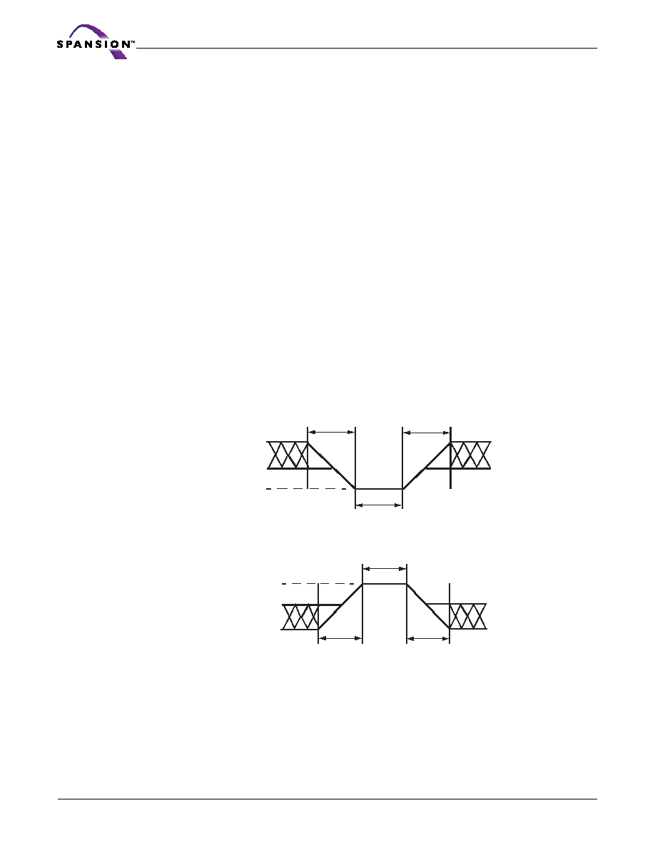
Figure 13.1 Maximum Negative Overshoot Waveform
Figure 13.2 Maximum Positive Overshoot Waveform
20 ns
+0.8 V
–0.5 V
20 ns
–2 V
20 ns
VCC +2.0 V
VCC+0.5 V
20 ns
2.0 V
相關(guān)PDF資料 |
PDF描述 |
|---|---|
| S29CL032J0RFFI110 | 1M X 32 FLASH 3.3V PROM, 48 ns, PBGA80 |
| S29CL032J0RFFN130 | 1M X 32 FLASH 3.3V PROM, 48 ns, PBGA80 |
| S29CL032J1JFAI110 | 1M X 32 FLASH 3.3V PROM, 54 ns, PBGA80 |
| S29CL032J1MFAN120 | 1M X 32 FLASH 3.3V PROM, 54 ns, PBGA80 |
| S29CL032J0PQAN102 | 1M X 32 FLASH 3.3V PROM, 54 ns, PQFP80 |
相關(guān)代理商/技術(shù)參數(shù) |
參數(shù)描述 |
|---|---|
| S29GL016A | 制造商:SPANSION 制造商全稱:SPANSION 功能描述:64 Megabit, 32 Megabit, and 16 Megabit 3.0-Volt only Page Mode Flash Memory Featuring 200 nm MirrorBit Process Technology |
| S29GL016A100BAI010 | 制造商:SPANSION 制造商全稱:SPANSION 功能描述:64 Megabit, 32 Megabit, and 16 Megabit 3.0-Volt only Page Mode Flash Memory Featuring 200 nm MirrorBit Process Technology |
| S29GL016A100BAI012 | 制造商:SPANSION 制造商全稱:SPANSION 功能描述:64 Megabit, 32 Megabit, and 16 Megabit 3.0-Volt only Page Mode Flash Memory Featuring 200 nm MirrorBit Process Technology |
| S29GL016A100BAI013 | 制造商:SPANSION 制造商全稱:SPANSION 功能描述:64 Megabit, 32 Megabit, and 16 Megabit 3.0-Volt only Page Mode Flash Memory Featuring 200 nm MirrorBit Process Technology |
| S29GL016A100BAIR10 | 制造商:SPANSION 制造商全稱:SPANSION 功能描述:64 Megabit, 32 Megabit, and 16 Megabit 3.0-Volt only Page Mode Flash Memory Featuring 200 nm MirrorBit Process Technology |
發(fā)布緊急采購,3分鐘左右您將得到回復(fù)。