- 您現(xiàn)在的位置:買賣IC網(wǎng) > PDF目錄192300 > S29GL128N11FAIVH0 (SPANSION LLC) 16M X 16 FLASH 3V PROM, 110 ns, PBGA64 PDF資料下載
參數(shù)資料
| 型號(hào): | S29GL128N11FAIVH0 |
| 廠商: | SPANSION LLC |
| 元件分類: | PROM |
| 英文描述: | 16M X 16 FLASH 3V PROM, 110 ns, PBGA64 |
| 封裝: | 10 X 13 MM, 1 MM PITCH, FBGA-64 |
| 文件頁數(shù): | 53/74頁 |
| 文件大小: | 1593K |
| 代理商: | S29GL128N11FAIVH0 |
第1頁第2頁第3頁第4頁第5頁第6頁第7頁第8頁第9頁第10頁第11頁第12頁第13頁第14頁第15頁第16頁第17頁第18頁第19頁第20頁第21頁第22頁第23頁第24頁第25頁第26頁第27頁第28頁第29頁第30頁第31頁第32頁第33頁第34頁第35頁第36頁第37頁第38頁第39頁第40頁第41頁第42頁第43頁第44頁第45頁第46頁第47頁第48頁第49頁第50頁第51頁第52頁當(dāng)前第53頁第54頁第55頁第56頁第57頁第58頁第59頁第60頁第61頁第62頁第63頁第64頁第65頁第66頁第67頁第68頁第69頁第70頁第71頁第72頁第73頁第74頁
May 1, 2006 S29GL-N_01_A0
S29GL-N
55
Data
She e t
12.7
DQ3: Sector Erase Timer
After writing a sector erase command sequence, the system may read DQ3 to determine whether or not
erasure has begun. (The sector erase timer does not apply to the chip erase command.) If additional sectors
are selected for erasure, the entire time-out also applies after each additional sector erase command. When
the time-out period is complete, DQ3 switches from a 0 to a 1. If the time between additional sector erase
commands from the system can be assumed to be less than 50 s, the system need not monitor DQ3. See
After the sector erase command is written, the system should read the status of DQ7 (Data# Polling) or DQ6
(Toggle Bit I) to ensure that the device has accepted the command sequence, and then read DQ3. If DQ3 is
1, the Embedded Erase algorithm has begun; all further commands (except Erase Suspend) are ignored until
the erase operation is complete. If DQ3 is 0, the device accepts additional sector erase commands. To
ensure the command is accepted, the system software should check the status of DQ3 prior to and following
each subsequent sector erase command. If DQ3 is high on the second status check, the last command might
not have been accepted.
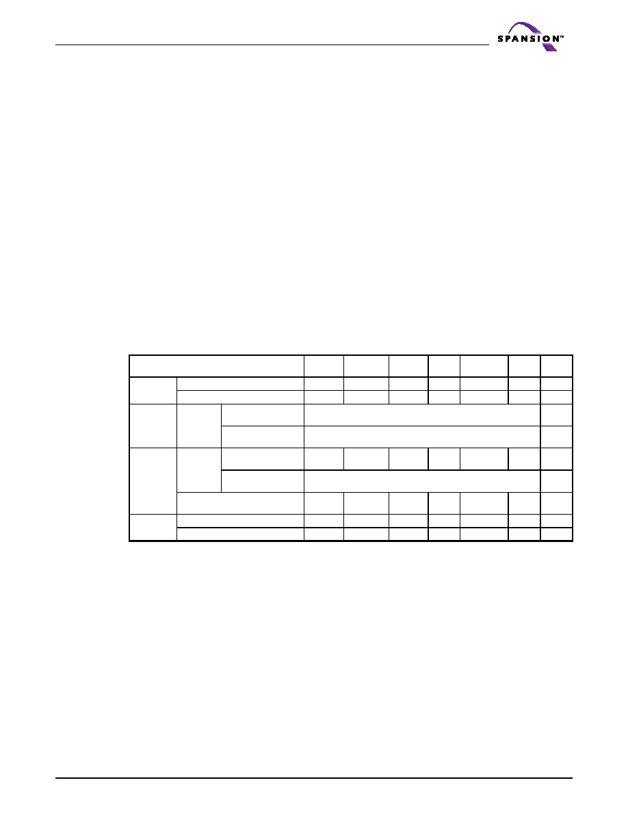
Table 12.1 on page 55 shows the status of DQ3 relative to the other status bits.
12.8
DQ1: Write-to-Buffer Abort
DQ1 indicates whether a Write-to-Buffer operation was aborted. Under these conditions DQ1 produces a 1.
The system must issue the Write-to-Buffer-Abort-Reset command sequence to return the device to reading
array data. See Write Buffer on page 12 for more details.
Notes
1. DQ5 switches to 1 when an Embedded Program, Embedded Erase, or Write-to-Buffer operation has exceeded the maximum timing
limits. Refer to DQ5: Exceeded Timing Limits on page 54 for more information.
2. DQ7 and DQ2 require a valid address when reading status information. Refer to the appropriate section for further details.
3. The Data# Polling algorithm should be used to monitor the last loaded write-buffer address location.
4. DQ1 switches to 1 when the device has aborted the write-to-buffer operation
Table 12.1 Write Operation Status
Status
DQ7
DQ6
DQ5
DQ3
DQ2
DQ1
RY/BY#
Standard
Mode
Embedded Program Algorithm
DQ7#
Toggle
0
N/A
No toggle
0
Embedded Erase Algorithm
0
Toggle
0
1
Toggle
N/A
0
Program
Suspend
Mode
Program-
Suspend
Read
Program-Suspended
Sector
Invalid (not allowed)
1
Non-Program
Suspended Sector
Data
1
Erase
Suspend
Mode
Erase-
Suspend
Read
Erase-Suspended
Sector
1
No toggle
0
N/A
Toggle
N/A
1
Non-Erase Suspended
Sector
Data
1
Erase-Suspend-Program
(Embedded Program)
DQ7#
Toggle
0
N/A
0
Write-to-
Buffer
Busy (Note 3)
DQ7#
Toggle
0
N/A
0
Abort (Note 4)
DQ7#
Toggle
0
N/A
1
0
相關(guān)PDF資料 |
PDF描述 |
|---|---|
| S29GL128N11FFIVH2 | 16M X 16 FLASH 3V PROM, 110 ns, PBGA64 |
| S29JL032J70TFI213 | 2M X 16 FLASH 3V PROM, 70 ns, PDSO48 |
| S29PL032J65BFI150 | 2M X 16 FLASH 3V PROM, 65 ns, PBGA56 |
| S29PL127J70BFI000 | 8M X 16 FLASH 3V PROM, 70 ns, PBGA80 |
| S29XS064R0PBHW010 | 4M X 16 FLASH 1.8V PROM, 80 ns, PBGA44 |
相關(guān)代理商/技術(shù)參數(shù) |
參數(shù)描述 |
|---|---|
| S29GL128N11FFA010 | 制造商:Spansion 功能描述: |
| S29GL128N11FFA013 | 制造商:Spansion 功能描述: |
| S29GL128N11FFI010 | 制造商:Spansion 功能描述:Flash - NOR IC |
| S29GL128N11FFI020 | 制造商:Spansion 功能描述: 制造商:Spansion 功能描述:Flash - NOR IC |
| S29GL128N11FFIIH0 | 制造商:Spansion 功能描述:NOR Flash Parallel 3V/3.3V 128Mbit 16M/8M x 8bit/16bit 110ns 64-Pin Fortified BGA Tray |
發(fā)布緊急采購,3分鐘左右您將得到回復(fù)。