- 您現(xiàn)在的位置:買賣IC網(wǎng) > PDF目錄385813 > SAA6713H (NXP Semiconductors N.V.) XGA dual input flat panel controller PDF資料下載
參數(shù)資料
| 型號(hào): | SAA6713H |
| 廠商: | NXP Semiconductors N.V. |
| 英文描述: | XGA dual input flat panel controller |
| 中文描述: | 雙輸入的XGA液晶控制器 |
| 文件頁數(shù): | 13/103頁 |
| 文件大?。?/td> | 521K |
| 代理商: | SAA6713H |
第1頁第2頁第3頁第4頁第5頁第6頁第7頁第8頁第9頁第10頁第11頁第12頁當(dāng)前第13頁第14頁第15頁第16頁第17頁第18頁第19頁第20頁第21頁第22頁第23頁第24頁第25頁第26頁第27頁第28頁第29頁第30頁第31頁第32頁第33頁第34頁第35頁第36頁第37頁第38頁第39頁第40頁第41頁第42頁第43頁第44頁第45頁第46頁第47頁第48頁第49頁第50頁第51頁第52頁第53頁第54頁第55頁第56頁第57頁第58頁第59頁第60頁第61頁第62頁第63頁第64頁第65頁第66頁第67頁第68頁第69頁第70頁第71頁第72頁第73頁第74頁第75頁第76頁第77頁第78頁第79頁第80頁第81頁第82頁第83頁第84頁第85頁第86頁第87頁第88頁第89頁第90頁第91頁第92頁第93頁第94頁第95頁第96頁第97頁第98頁第99頁第100頁第101頁第102頁第103頁
2004 Apr 05
13
Philips Semiconductors
Product specification
XGA dual input flat panel controller
SAA6713H
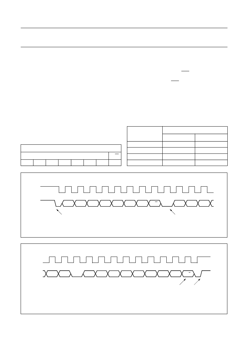
If the write mode was selected, the bus master sends a
byte containing the starting subaddress and then a series
of data bytes. In case the read mode was selected, the
addressed slave returns a series of data bytes. A read
transfer is preceded by a write transfer that transmits the
starting subaddress.
Data transfers are aborted by the stop condition, when
SDA is changed by the master from LOW-to-HIGH level
when SCL is at HIGH-level (see Fig.4).
7.1.2.3
I
2
C-bus device address
Bits A0 and A1 of the I
2
C-bus device address are
externally selected by two input pins CSG2/A0
and CSG4/A1. The device address (byte) of the
SAA6713H is shown in Table 4.
Table 4
I
2
C-bus device address byte
The four possible I
2
C-bus device addresses are selected
via resistor strapping at pins CSG2/A0 and CSG4/A1
(see Table 5).
During the hardware reset (pin RST = LOW),
pins CSG2/A0 and CSG4/A1 are 3-stated. Their status at
the trailing edge of signal RST will latch and determine the
device address. Pull-up and pull-down resistors (4.7 k
suggested) select the address. An internal pull-down
resistance of approximately 100 k
is provided and
eliminates potentially the need for any external strapping
resistor. After reset, the pins carry the output of the
programmable signal generators.
Table 5
Device address selection
MSB
LSB
DEVICE ADDRESS BITS
R/W
0
1
1
1
0
A1
A0
0/1
I
2
C-BUS DEVICE
ADDRESS
STRAPPING RESISTOR
PIN CSG4/A1
PIN CSG2/A0
70H
72H
74H
76H
pull-down
pull-down
pull-up
pull-up
pull-down
pull-up
pull-down
pull-up
Fig.3 Start of a data transfer.
handbook, full pagewidth
MHB248
SDA
A4
A1
A2
A3
A6
A5
ACK
R/W
A0
R5
R7
R6
START condition
acknowledge
Fig.4 End of a data transfer.
handbook, full pagewidth
MHB249
SDA
D7
D4
D5
D6
D1
D0
ACK
D2
D3
A/A
D1
D0
STOP condition
acknowledge/
not acknowledge
相關(guān)PDF資料 |
PDF描述 |
|---|---|
| SAA7110 | Digital Multistandard Colour Decoder(數(shù)字多標(biāo)準(zhǔn)彩色譯碼器) |
| SAA7111 | Video Input Processor VIP |
| SAA7120H | Digital video encoder |
| SAA7152 | Digital Video Comb Filter DCF |
| SAA7184 | Digital Video Encoders DENC2-M6 |
相關(guān)代理商/技術(shù)參數(shù) |
參數(shù)描述 |
|---|---|
| SAA6713H/V1 | 制造商:PHILIPS 制造商全稱:NXP Semiconductors 功能描述:XGA dual input flat panel controller |
| SAA6721 | 制造商:PHILIPS 制造商全稱:NXP Semiconductors 功能描述:SXGA RGB to TFT graphics engine |
| SAA6721E | 制造商:PHILIPS 制造商全稱:NXP Semiconductors 功能描述:SXGA RGB to TFT graphics engine |
| SAA6750 | 制造商:PHILIPS 制造商全稱:NXP Semiconductors 功能描述:Encoder for MPEG2 image recording EMPIRE |
| SAA6750H | 制造商:PHILIPS 制造商全稱:NXP Semiconductors 功能描述:Encoder for MPEG2 image recording EMPIRE |
發(fā)布緊急采購,3分鐘左右您將得到回復(fù)。