- 您現(xiàn)在的位置:買賣IC網(wǎng) > PDF目錄372113 > SAA7109A (NXP Semiconductors N.V.) HD-CODEC PDF資料下載
參數(shù)資料
| 型號(hào): | SAA7109A |
| 廠商: | NXP Semiconductors N.V. |
| 元件分類: | Codec |
| 英文描述: | HD-CODEC |
| 中文描述: | 高清解碼器 |
| 文件頁數(shù): | 128/197頁 |
| 文件大小: | 983K |
| 代理商: | SAA7109A |
第1頁第2頁第3頁第4頁第5頁第6頁第7頁第8頁第9頁第10頁第11頁第12頁第13頁第14頁第15頁第16頁第17頁第18頁第19頁第20頁第21頁第22頁第23頁第24頁第25頁第26頁第27頁第28頁第29頁第30頁第31頁第32頁第33頁第34頁第35頁第36頁第37頁第38頁第39頁第40頁第41頁第42頁第43頁第44頁第45頁第46頁第47頁第48頁第49頁第50頁第51頁第52頁第53頁第54頁第55頁第56頁第57頁第58頁第59頁第60頁第61頁第62頁第63頁第64頁第65頁第66頁第67頁第68頁第69頁第70頁第71頁第72頁第73頁第74頁第75頁第76頁第77頁第78頁第79頁第80頁第81頁第82頁第83頁第84頁第85頁第86頁第87頁第88頁第89頁第90頁第91頁第92頁第93頁第94頁第95頁第96頁第97頁第98頁第99頁第100頁第101頁第102頁第103頁第104頁第105頁第106頁第107頁第108頁第109頁第110頁第111頁第112頁第113頁第114頁第115頁第116頁第117頁第118頁第119頁第120頁第121頁第122頁第123頁第124頁第125頁第126頁第127頁當(dāng)前第128頁第129頁第130頁第131頁第132頁第133頁第134頁第135頁第136頁第137頁第138頁第139頁第140頁第141頁第142頁第143頁第144頁第145頁第146頁第147頁第148頁第149頁第150頁第151頁第152頁第153頁第154頁第155頁第156頁第157頁第158頁第159頁第160頁第161頁第162頁第163頁第164頁第165頁第166頁第167頁第168頁第169頁第170頁第171頁第172頁第173頁第174頁第175頁第176頁第177頁第178頁第179頁第180頁第181頁第182頁第183頁第184頁第185頁第186頁第187頁第188頁第189頁第190頁第191頁第192頁第193頁第194頁第195頁第196頁第197頁
2004 Jun 29
128
Philips Semiconductors
Product specification
HD-CODEC
SAA7108AE; SAA7109AE
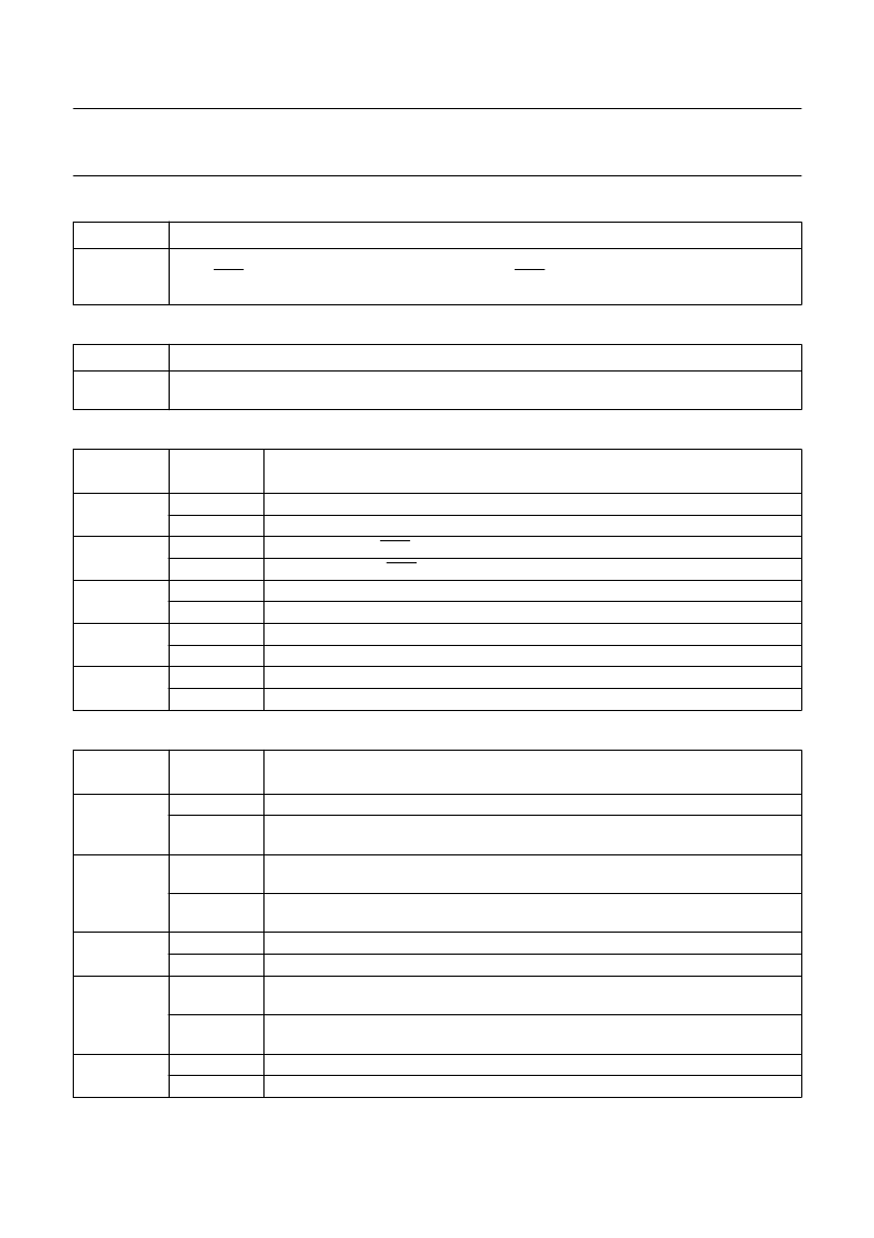
Table 110
Subaddresses 93H and 94H
Table 111
Subaddresses 95H and 96H
Table 112
Subaddress 96H
Table 113
Subaddress 97H
DATA BYTE
DESCRIPTION
YOFSE
vertical offset in even field; defines (in the even field) the number of lines from VSVGC to first line with
active CBO; if no LUT data is requested, the first active CBO will be output at YOFSE + 2; usually,
YOFSE = YOFSO with the exception of extreme vertical downscaling and interlacing
DATA BYTE
DESCRIPTION
YPIX
defines the number of requested input lines from the feeding device;
number of requested lines = YPIX + YOFSE
YOFSO
DATA BYTE
LOGIC
LEVEL
DESCRIPTION
EFS
0
1
0
1
0
1
0
1
0
1
frame sync signal at pin FSVGC ignored in slave mode
frame sync signal at pin FSVGC accepted in slave mode
normal polarity of CBO signal (HIGH during active video)
inverted polarity of CBO signal (LOW during active video)
the SAA7108AE; SAA7109AE is timing master to the graphics controller
the SAA7108AE; SAA7109AE is timing slave to the graphics controller
if hardware cursor insertion is active, set LOW for non-interlaced input signals
if hardware cursor insertion is active, set HIGH for interlaced input signals
luminance sharpness booster disabled
luminance sharpness booster enabled
PCBN
SLAVE
ILC
YFIL
DATA BYTE
LOGIC
LEVEL
DESCRIPTION
HFS
0
1
horizontal sync is directly derived from input signal (slave mode) at pin HSVGC
horizontal sync is derived from a frame sync signal (slave mode) at pin FSVGC (only if
EFS is set HIGH)
vertical sync (field sync) is directly derived from input signal (slave mode) at
vertical sync (field sync) is derived from a frame sync signal (slave mode) at
pin FSVGC (only if EFS is set HIGH)
pin FSVGC is switched to input
pin FSVGC is switched to active output
polarity of signal at pin FSVGC in output mode (master mode) is active HIGH; rising
edge of the input signal is used in slave mode
polarity of signal at pin FSVGC in output mode (master mode) is active LOW; falling
edge of the input signal is used in slave mode
pin VSVGC is switched to input
pin VSVGC is switched to active output
VFS
0
1
OFS
0
1
0
PFS
1
OVS
0
1
相關(guān)PDF資料 |
PDF描述 |
|---|---|
| SAA7109AE | HD-CODEC |
| SAA7110A | Digital Multistandard Colour Decoder(數(shù)字多標(biāo)準(zhǔn)彩色譯碼器) |
| SAA7111A | Enhanced Video Input Processor EVIP |
| SAA7111AH | Enhanced Video Input Processor EVIP |
| SAA7111AHZ | GT 13C 13#16 SKT PLUG |
相關(guān)代理商/技術(shù)參數(shù) |
參數(shù)描述 |
|---|---|
| SAA7109AE | 制造商:PHILIPS 制造商全稱:NXP Semiconductors 功能描述:HD-CODEC |
| SAA7109AE/V1,518 | 功能描述:視頻 IC HD- VIDEO CODEC RoHS:否 制造商:Fairchild Semiconductor 工作電源電壓:5 V 電源電流:80 mA 最大工作溫度:+ 85 C 封裝 / 箱體:TSSOP-28 封裝:Reel |
| SAA7109AE/V1,557 | 功能描述:視頻 IC HD- VIDEO CODEC RoHS:否 制造商:Fairchild Semiconductor 工作電源電壓:5 V 電源電流:80 mA 最大工作溫度:+ 85 C 封裝 / 箱體:TSSOP-28 封裝:Reel |
| SAA7109AE/V1/G | 功能描述:視頻 IC PC CODEC (W/OUT MICROVISION) RoHS:否 制造商:Fairchild Semiconductor 工作電源電壓:5 V 電源電流:80 mA 最大工作溫度:+ 85 C 封裝 / 箱體:TSSOP-28 封裝:Reel |
| SAA7109AE/V1/G,518 | 功能描述:視頻 IC SAA7109AE/LBGA156/REEL13DP//V1 RoHS:否 制造商:Fairchild Semiconductor 工作電源電壓:5 V 電源電流:80 mA 最大工作溫度:+ 85 C 封裝 / 箱體:TSSOP-28 封裝:Reel |
發(fā)布緊急采購,3分鐘左右您將得到回復(fù)。