- 您現(xiàn)在的位置:買(mǎi)賣(mài)IC網(wǎng) > PDF目錄376341 > SCM69C433 (Motorola, Inc.) A Flexible Content-Addressable Memory (16K x 64 CAM)(1M內(nèi)容可尋址存儲(chǔ)器) PDF資料下載
參數(shù)資料
| 型號(hào): | SCM69C433 |
| 廠(chǎng)商: | Motorola, Inc. |
| 英文描述: | A Flexible Content-Addressable Memory (16K x 64 CAM)(1M內(nèi)容可尋址存儲(chǔ)器) |
| 中文描述: | 一個(gè)靈活的內(nèi)容尋址存儲(chǔ)器(16K的× 64 CAM)的(100萬(wàn)內(nèi)容可尋址存儲(chǔ)器) |
| 文件頁(yè)數(shù): | 19/22頁(yè) |
| 文件大小: | 167K |
| 代理商: | SCM69C433 |
第1頁(yè)第2頁(yè)第3頁(yè)第4頁(yè)第5頁(yè)第6頁(yè)第7頁(yè)第8頁(yè)第9頁(yè)第10頁(yè)第11頁(yè)第12頁(yè)第13頁(yè)第14頁(yè)第15頁(yè)第16頁(yè)第17頁(yè)第18頁(yè)當(dāng)前第19頁(yè)第20頁(yè)第21頁(yè)第22頁(yè)

MCM69C433
SCM69C433
19
MOTOROLA FAST SRAM
TEST ACCESS PORT PINS
TCK — TEST CLOCK (INPUT)
Clocks all TAP events. All inputs are captured on the rising
edge of TCK and all outputs propagate from the falling edge
of TCK.
TMS — TEST MODE SELECT (INPUT)
The TMS input is sampled on the rising edge of TCK. This
is the command input for the TAP controller state machine.
An undriven TMS input will produce the same result as a
logic 1 input level.
TDI — TEST DATA IN (INPUT)
The TDI input is sampled on the rising edge of TCK. This is
the input side of the serial registers placed between TDI and
TDO. The register placed between TDI and TDO is deter-
mined by the state of the TAP controller state machine and
the instruction that is currently loaded in the TAP instruction
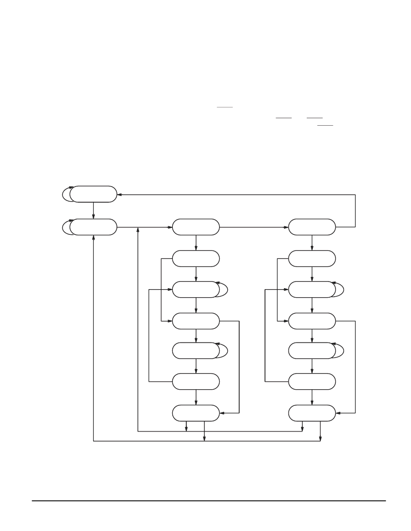
register (see Figure 5). An undriven TDI pin will produce the
same result as a logic 1 input level.
TDO — TEST DATA OUT (OUTPUT)
Output that is active depending on the state of the TAP
state machine (see Figure 5). Output changes in response to
the falling edge of TCK. This is the output side of the serial
registers placed between TDI and TDO.
TRST — TAP RESET
This device has a TRST pin. TRST is optional in IEEE
1149.1. Asserting the asynchronous TRST places the TAP
controller in test–logic reset state. Test–logic reset state can
also be entered by holding TMS high for five rising edges of
TCK. This type of reset does not affect the operation of the
system logic.
SHIFT–DR
EXIT1–IR
SELECT IR–SCAN
PAUSE–IR
TEST–LOGIC
RESET
EXIT1–DR
UPDATE–IR
CAPTURE–IR
SHIFT–IR
EXIT2–IR
0
RUN–TEST/
IDLE
1
PAUSE 2–DR
EXIT2–DR
PAUSE 1–DR
CAPTURE–DR
0
0
0
0
0
0
0
0
1
1
1
1
1
1
1
1
1
0
0
0
1
1
1
0
0
0
1
1
1
SELECT DR–SCAN
0
NOTE: The value adjacent to each state transition represents the signal present at TMS at the rising edge of TCK.
Figure 5. TAP Controller State Diagram
相關(guān)PDF資料 |
PDF描述 |
|---|---|
| SD1012-03 | Side Door Adapter |
| SD1013-03 | RF MICROWAVE TRANSISTORS 108-152 MHZ APPLICATIONS |
| SD1013-3 | RF & MICROWAVE TRANSISTORS 108-152 MHz APPLICATIONS |
| SD1014-02 | PTSE 8C 8#20 PIN RECP |
| SD1014 | RF & MICROWAVE TRANSISTORS |
相關(guān)代理商/技術(shù)參數(shù) |
參數(shù)描述 |
|---|---|
| SCM69C433TQ15 | 制造商:MOTOROLA 制造商全稱(chēng):Motorola, Inc 功能描述:16K x 64 CAM |
| SCM69C433TQ15R | 制造商:MOTOROLA 制造商全稱(chēng):Motorola, Inc 功能描述:16K x 64 CAM |
| SCM8245ALVV400D | 制造商:Freescale Semiconductor 功能描述:INTEGEATED HOST PROC |
| SCM8245ALZU400D | 制造商:Freescale Semiconductor 功能描述:INTEGRATED HOST PROC |
| SCM9B-3000 | 制造商:未知廠(chǎng)家 制造商全稱(chēng):未知廠(chǎng)家 功能描述:Computer-to-Analog Output Modules |
發(fā)布緊急采購(gòu),3分鐘左右您將得到回復(fù)。