- 您現(xiàn)在的位置:買賣IC網(wǎng) > PDF目錄98144 > ST62P35BQ1/XXX (STMICROELECTRONICS) 8-BIT, MROM, 8 MHz, MICROCONTROLLER, PQFP52 PDF資料下載
參數(shù)資料
| 型號: | ST62P35BQ1/XXX |
| 廠商: | STMICROELECTRONICS |
| 元件分類: | 微控制器/微處理器 |
| 英文描述: | 8-BIT, MROM, 8 MHz, MICROCONTROLLER, PQFP52 |
| 封裝: | PLASTIC, QFP-52 |
| 文件頁數(shù): | 47/82頁 |
| 文件大小: | 617K |
| 代理商: | ST62P35BQ1/XXX |
第1頁第2頁第3頁第4頁第5頁第6頁第7頁第8頁第9頁第10頁第11頁第12頁第13頁第14頁第15頁第16頁第17頁第18頁第19頁第20頁第21頁第22頁第23頁第24頁第25頁第26頁第27頁第28頁第29頁第30頁第31頁第32頁第33頁第34頁第35頁第36頁第37頁第38頁第39頁第40頁第41頁第42頁第43頁第44頁第45頁第46頁當(dāng)前第47頁第48頁第49頁第50頁第51頁第52頁第53頁第54頁第55頁第56頁第57頁第58頁第59頁第60頁第61頁第62頁第63頁第64頁第65頁第66頁第67頁第68頁第69頁第70頁第71頁第72頁第73頁第74頁第75頁第76頁第77頁第78頁第79頁第80頁第81頁第82頁

51/82
ST62T35B/E35B
CONTROL REGISTERS (Cont’d)
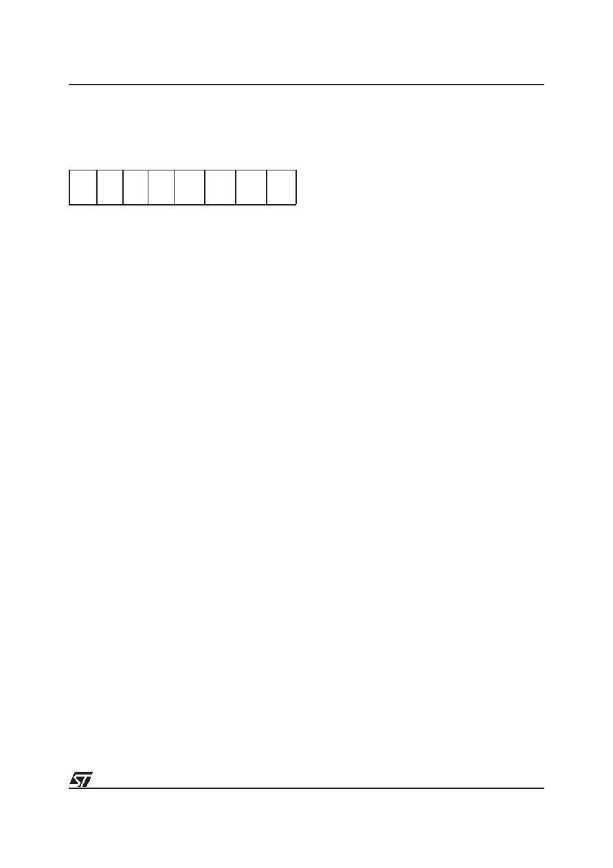
Status Control Register 4 (SCR4)
Address: E3h - Read/Write/Clear only
Bit7- Bit4 = Reserved, set to 0.
Bit 3 = OVFPOL.
Overflow Output Polarity. This bit
defines the polarity for the Overflow Output OVF.
When 0, OVF is set on every overflow event if en-
abled in Set mode (OVFEN = 1, OVFMD = 0). The
reset state of OVF is 0.
When 1, OVF is reset on every overflow event if
enabled in Set mode.
The reset state of OVF is 1.
Bit 2 = OVFEN.
Overflow Output Enable. This bit
enables the Overflow output OVF. When 0 the
Overflow output is disabled: if OVFPOL = 0, the
state of OVF is 0, if OVFPOL = 1, the state of
OVF = 1.The Overflow Output is enabled when
this bit = 1, it must be set to use the OVF output.
Bit 1 = PWMPOL.
PWM Output Polarity. This bit
defines the polarity for the PWM Output PWM.
When 0, PWM is set on every Masked-Counter
Zero event and is reset on a Masked-Compare if
enabled in Set/Reset mode (PWMEN = 1, PWM-
MD = 0).
The reset state of PWM pin is 0 When 1, OVF is
set on every Masked-Compare event and is reset
on a Masked-Counter Zero event if enabled in
Set/Reset mode (PWMEN = 1, PWMMD = 0).
The reset state of PWM is 1.
Bit 0 = PWMEN.
PWM Output Enable. This bit en-
ables the PWM output PWM. When 0 the PWM
output is disabled: if PWMPOL = 0, the state of
PWM is 0, if PWMPOL = 1, the state of PWM = 1.
The PWM Output is enabled when this bit = 1, it
must be set to use the PWM output.
Notes:
A Masked-Compare is the logical AND of the
Mask Register MASK with the Counter Register
CT, compared with the logical AND of the com-
pare
Register
CMP:
[(MASK
&
CT)
=
(MASK&CMP)].
A Masked-Counter Zero is the logical AND of the
Mask Register MASK with the Counter Register
CT, compared with zero: [(MASK & CT) = 0000h].
4.3.6 16-BIT REGISTERS
Note: Care must be taken when using single-bit
instructions (RES/SET/INC/DEC) 16-bit registers
(RLCP, CP, CMP, MSK) since these instructions
imply a READ-MODIFY-WRITE operation on the
register. As the ST6 is based on a 8-bit architec-
ture, to write a 16-bit register, the high byte must
be written first to an intermediate register (latch
register) and the whole 16-bit register is loaded at
the same time as the low byte is written. A WRITE
operation of the HIGH byte is performed on the in-
termediate register (latch register) but a READ op-
eration of the HIGH byte is directly performed on
the 16-bit register (last loaded value). As a conse-
quence, it is always mandatory to write the LOW
byte before any single-bit instruction on the HIGH
byte in order to load the value set in the intermedi-
ate register to the 16-bit register (refresh the 16-bit
register).
Example:
The following sequence is NOT GOOD:
ldi t16cmph, 055h
ldi t16cmpl, 000h
; t16cm p (16-bit register )=55 00h
ldi t16cmph, 0AAh
; t16cm p (16-bit register )=55 00h
inc t16cmph
; t16cm p (16-bit register )=55 00h
ldi t16cmpl, 000h
; t16cm p (16-bit register )=56 00h
; and NOT AB00h
The CORRECT sequence is:
ldi t16cmph, 055h
ldi t16cmpl, 000h
; t16cm p (16-bit register )=55 00h
ldi t16cmph, 0AAh
; t16cm p (16-bit register )=55 00h
ldi t16cmpl, 000h
; t16cm p (16-bit register )=AA 00h
inc t16cmph
; t16cm p (16-bit register )=AA 00h
ldi t16cmpl, 000h
;t16cmp (16-bit regis ter) =AB0 0h
70
Res.
Res. Res. Res.
OVFPO
L
OVFEN PMPOL
PWME
N
50
相關(guān)PDF資料 |
PDF描述 |
|---|---|
| ST6235BQ1/XXX | 8-BIT, MROM, 8 MHz, MICROCONTROLLER, PQFP52 |
| ST62P45BQ6/XXX | 8-BIT, MROM, 8 MHz, MICROCONTROLLER, PQFP52 |
| ST62T03CM6E | 8-BIT, OTPROM, 8 MHz, MICROCONTROLLER, PDSO16 |
| ST62T10BM6 | 8-BIT, OTPROM, 8 MHz, MICROCONTROLLER, PDSO20 |
| ST62T25BB6 | 8-BIT, OTPROM, 8 MHz, MICROCONTROLLER, PDIP28 |
相關(guān)代理商/技術(shù)參數(shù) |
參數(shù)描述 |
|---|---|
| ST62P52C | 制造商:STMicroelectronics 功能描述: |
| ST62P62CM6/MOMTR | 制造商:STMicroelectronics 功能描述: |
| ST62P62CM6/MPITR | 制造商:STMicroelectronics 功能描述: |
| ST62P62CM6/MSATR | 制造商:STMicroelectronics 功能描述: |
| ST62P62CN6/MMMTR | 制造商:STMicroelectronics 功能描述: |
發(fā)布緊急采購,3分鐘左右您將得到回復(fù)。