- 您現(xiàn)在的位置:買(mǎi)賣(mài)IC網(wǎng) > PDF目錄98144 > ST62P45BQ6/XXX (STMICROELECTRONICS) 8-BIT, MROM, 8 MHz, MICROCONTROLLER, PQFP52 PDF資料下載
參數(shù)資料
| 型號(hào): | ST62P45BQ6/XXX |
| 廠商: | STMICROELECTRONICS |
| 元件分類: | 微控制器/微處理器 |
| 英文描述: | 8-BIT, MROM, 8 MHz, MICROCONTROLLER, PQFP52 |
| 封裝: | PLASTIC, QFP-52 |
| 文件頁(yè)數(shù): | 46/72頁(yè) |
| 文件大小: | 514K |
| 代理商: | ST62P45BQ6/XXX |
第1頁(yè)第2頁(yè)第3頁(yè)第4頁(yè)第5頁(yè)第6頁(yè)第7頁(yè)第8頁(yè)第9頁(yè)第10頁(yè)第11頁(yè)第12頁(yè)第13頁(yè)第14頁(yè)第15頁(yè)第16頁(yè)第17頁(yè)第18頁(yè)第19頁(yè)第20頁(yè)第21頁(yè)第22頁(yè)第23頁(yè)第24頁(yè)第25頁(yè)第26頁(yè)第27頁(yè)第28頁(yè)第29頁(yè)第30頁(yè)第31頁(yè)第32頁(yè)第33頁(yè)第34頁(yè)第35頁(yè)第36頁(yè)第37頁(yè)第38頁(yè)第39頁(yè)第40頁(yè)第41頁(yè)第42頁(yè)第43頁(yè)第44頁(yè)第45頁(yè)當(dāng)前第46頁(yè)第47頁(yè)第48頁(yè)第49頁(yè)第50頁(yè)第51頁(yè)第52頁(yè)第53頁(yè)第54頁(yè)第55頁(yè)第56頁(yè)第57頁(yè)第58頁(yè)第59頁(yè)第60頁(yè)第61頁(yè)第62頁(yè)第63頁(yè)第64頁(yè)第65頁(yè)第66頁(yè)第67頁(yè)第68頁(yè)第69頁(yè)第70頁(yè)第71頁(yè)第72頁(yè)
50/72
ST62T45B/E45B
LCD CONTROLLER-DRIVER (Continued)
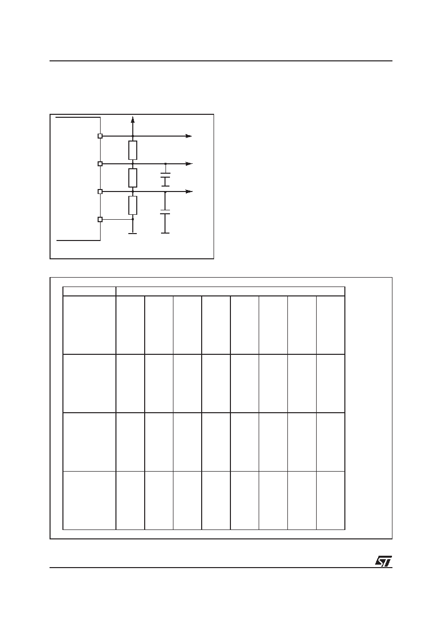
Figure 29. Typical Network to connect to VLCD
pins if VLCD
≤ 4.5V
Typical External resistances values are in the
range of 100 k
to 150 k. External capacitances
in the range of 10 to 47 nF can be added to VLCD
2/3 and VLCD 1/3 pins and to VLCD if the VLCD con-
nection is highly impedant.
4.5.3 LCD RAM
LCD RAM is organised as a LCD panel with a ma-
trix architecture. Each bit of its content is logically
mapped to a physical element of the display panel
addressed by a couple (Segment;Common). If a
bit is set, the relevant element of the LCD matrix is
turned-on. On the contrary, an element remains
turned-off as long the associated bit within the
LCD RAM is kept cleared.
After a reset, the LCD RAM is not initialised and
contain arbitrary information.
If the choosen multiplexing ratio does not use
some common plates, corresponding RAM ad-
dresses are free for general purpose data storage.
Figure 30. Addressing Map of the LCD RAM
VLCD
R
VLCD1/3
VSS
VLCD2/3
C
R: 100k
R
C
C: 47nF
VR01840
RAM Address
MSB
LSB
E0
E1
E2
E3
E4
E5
S8
S16
S24
S32
S40
S48
S7
S15
S23
S31
S39
S47
S6
S14
S22
S30
S38
S46
S5
S13
S21
S29
S37
S45
S4
S12
S20
S28
S36
S44
NA
S11
S19
S27
S35
S43
NA
S10
S18
S26
S34
S42
NA
S9
S17
S25
S33
S41
COM1
E6
E7
E8
E9
EA
EB
S8
S16
S24
S32
S40
S48
S7
S15
S23
S31
S39
S47
S6
S14
S22
S30
S38
S46
S5
S13
S21
S29
S37
S45
S4
S12
S20
S28
S36
S44
NA
S11
S19
S27
S35
S43
NA
S10
S18
S26
S34
S42
NA
S9
S17
S25
S33
S41
COM2
EC
ED
EE
EF
F0
F1
S8
S16
S24
S32
S40
S48
S7
S15
S23
S31
S39
S47
S6
S14
S22
S30
S38
S46
S5
S13
S21
S29
S37
S45
S4
S12
S20
S28
S36
S44
NA
S11
S19
S27
S35
S43
NA
S10
S18
S26
S34
S42
NA
S9
S17
S25
S33
S41
COM3
F2
F3
F4
F5
F6
F7
S8
S16
S24
S32
S40
S48
S7
S15
S23
S31
S39
S47
S6
S14
S22
S30
S38
S46
S5
S13
S21
S29
S37
S45
S4
S12
S20
S28
S36
S44
NA
S11
S19
S27
S35
S43
NA
S10
S18
S26
S34
S42
NA
S9
S17
S25
S33
S41
COM4
49
相關(guān)PDF資料 |
PDF描述 |
|---|---|
| ST62T03CM6E | 8-BIT, OTPROM, 8 MHz, MICROCONTROLLER, PDSO16 |
| ST62T10BM6 | 8-BIT, OTPROM, 8 MHz, MICROCONTROLLER, PDSO20 |
| ST62T25BB6 | 8-BIT, OTPROM, 8 MHz, MICROCONTROLLER, PDIP28 |
| ST62T20BB6 | 8-BIT, OTPROM, 8 MHz, MICROCONTROLLER, PDIP20 |
| ST62T18CB6 | 8-BIT, OTPROM, 8 MHz, MICROCONTROLLER, PDIP20 |
相關(guān)代理商/技術(shù)參數(shù) |
參數(shù)描述 |
|---|---|
| ST62P52C | 制造商:STMicroelectronics 功能描述: |
| ST62P62CM6/MOMTR | 制造商:STMicroelectronics 功能描述: |
| ST62P62CM6/MPITR | 制造商:STMicroelectronics 功能描述: |
| ST62P62CM6/MSATR | 制造商:STMicroelectronics 功能描述: |
| ST62P62CN6/MMMTR | 制造商:STMicroelectronics 功能描述: |
發(fā)布緊急采購(gòu),3分鐘左右您將得到回復(fù)。