- 您現(xiàn)在的位置:買賣IC網(wǎng) > PDF目錄373606 > TC9325F (Toshiba Corporation) Single-Chip DTS Microcontroller (DTS-20) PDF資料下載
參數(shù)資料
| 型號(hào): | TC9325F |
| 廠商: | Toshiba Corporation |
| 英文描述: | Single-Chip DTS Microcontroller (DTS-20) |
| 中文描述: | 單芯片微丘(丘- 20) |
| 文件頁數(shù): | 94/101頁 |
| 文件大小: | 1802K |
| 代理商: | TC9325F |
第1頁第2頁第3頁第4頁第5頁第6頁第7頁第8頁第9頁第10頁第11頁第12頁第13頁第14頁第15頁第16頁第17頁第18頁第19頁第20頁第21頁第22頁第23頁第24頁第25頁第26頁第27頁第28頁第29頁第30頁第31頁第32頁第33頁第34頁第35頁第36頁第37頁第38頁第39頁第40頁第41頁第42頁第43頁第44頁第45頁第46頁第47頁第48頁第49頁第50頁第51頁第52頁第53頁第54頁第55頁第56頁第57頁第58頁第59頁第60頁第61頁第62頁第63頁第64頁第65頁第66頁第67頁第68頁第69頁第70頁第71頁第72頁第73頁第74頁第75頁第76頁第77頁第78頁第79頁第80頁第81頁第82頁第83頁第84頁第85頁第86頁第87頁第88頁第89頁第90頁第91頁第92頁第93頁當(dāng)前第94頁第95頁第96頁第97頁第98頁第99頁第100頁第101頁
TC9325F
2002-05-14
94
○
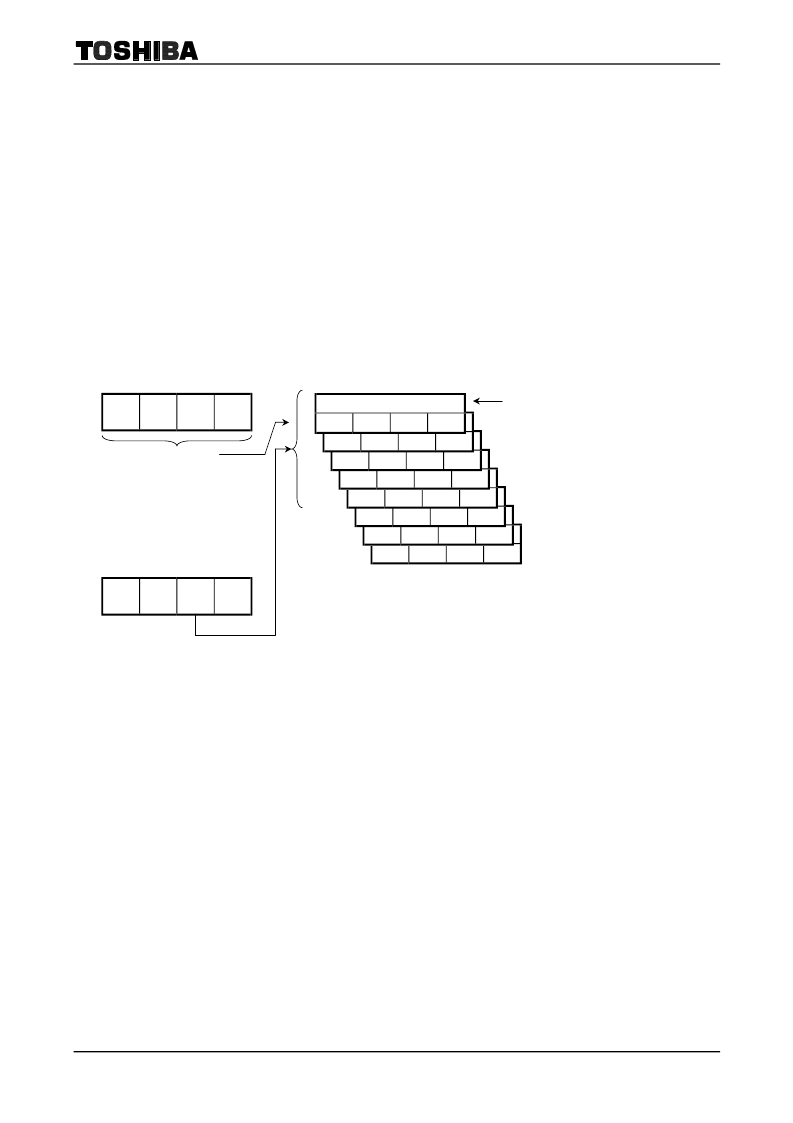
Output Ports (Also Function as LCD Driver Pins)
The output port includes 30 CMOS output ports, which also function as the LCD driver. The LCD OFF
bit is used to switch the port to an output port. Setting the LCD OFF bit to 1 sets the port to an output port.
The data output to the output port can be accessed by the OUT2 instruction with the operand [CN
=
CH].
These data can be divided/indirectly specified and set using the data selection port (
φ
L2B). First set the
data for the segment data port you wish to set, then access the corresponding data port.
The data selection port is incremented by 1 every time a general-purpose output data port (
φ
L2C) is
accessed. Accordingly, after setting the data selection port, the data can be repeatedly set.
In OT1 to OT20, output data can be incremented by 1 in one instruction by using the OT count UP bit.
Therefore, OT1 to OT20 can be used for the address signal output when using external memory.
Note: The data selection port is automatically incremented by 1 whenever
φ
L2C,
φ
L2D,
φ
L2E,
φ
L2F,
φ
L3B, or
φ
K3B on the I/O map are accessed.
Note: Setting the OT count UP bit to 0 sets no count up.
Note: See the LCD driver section.
Y1
Y4
Y8
DAL
1
7 OT29 OT30
*
*
Y2
Y4
Y8
DAL
OT2Y2
1
6 OT25 OT26 OT27 OT28
Y2
Y4
Y8
DAL
1
5
O21
φ
L2C
Y1
Y4
Y8
4 OT1Y1
φ
L2B
Y1
Y2
Y4
Y8
SEL1 SEL2 SEL4 SEL8
Data selection
Setting the LCD OFF bit to 1 sets the
segment output data to output port data.
Y2
Y4
Y8
DAL
OT1Y2
1
3 OT1L/K3B
φ
L3A
Y1
Y2
Y4
Y8
OT
count
up
OT1 to OT20 are counted up (incremented by 1)
whenever this bit is set to 1.
The OT1 bit is the lowest bit and OT20 the highest. The
countup starts from OT1.
φ
L/Output port data
Y1
Y2
Y4
Y8
DAL
OT6
1
2
OT9
Y2
Y4
Y8
DAL
OT2
1
1
OT5
OT7
OT8
φ
L2C
Y1
Y2
Y4
Y8
0
OT1
OT3
OT4
相關(guān)PDF資料 |
PDF描述 |
|---|---|
| TC9327 | DTS MICROCONTROLLER |
| TC9327F | DTS MICROCONTROLLER |
| TC9331 | AUDIO DIGITAL SIGNAL PROCESSOR |
| TC9331F | AUDIO DIGITAL SIGNAL PROCESSOR |
| TC9332 | AUDIO DIGITAL SIGNAL PROCESSOR |
相關(guān)代理商/技術(shù)參數(shù) |
參數(shù)描述 |
|---|---|
| TC9327 | 制造商:TOSHIBA 制造商全稱:Toshiba Semiconductor 功能描述:DTS MICROCONTROLLER |
| TC9327BFG | 制造商:TOSHIBA 制造商全稱:Toshiba Semiconductor 功能描述:DTS Microcontroller (DTS-21) |
| TC9327F | 制造商:TOSHIBA 制造商全稱:Toshiba Semiconductor 功能描述:DTS MICROCONTROLLER |
| TC9328AF | 制造商:TOSHIBA 制造商全稱:Toshiba Semiconductor 功能描述:Portable Audio DTS Controller (DTS-21) |
| TC9328AF_04 | 制造商:TOSHIBA 制造商全稱:Toshiba Semiconductor 功能描述:Portable Audio DTS Controller (DTS-21) |
發(fā)布緊急采購,3分鐘左右您將得到回復(fù)。