- 您現(xiàn)在的位置:買賣IC網(wǎng) > PDF目錄373629 > TEA2028-TEA2029 (意法半導(dǎo)體) APPLICATION NOTE PDF資料下載
參數(shù)資料
| 型號: | TEA2028-TEA2029 |
| 廠商: | 意法半導(dǎo)體 |
| 英文描述: | APPLICATION NOTE |
| 中文描述: | 應(yīng)用筆記 |
| 文件頁數(shù): | 25/47頁 |
| 文件大小: | 532K |
| 代理商: | TEA2028-TEA2029 |
第1頁第2頁第3頁第4頁第5頁第6頁第7頁第8頁第9頁第10頁第11頁第12頁第13頁第14頁第15頁第16頁第17頁第18頁第19頁第20頁第21頁第22頁第23頁第24頁當(dāng)前第25頁第26頁第27頁第28頁第29頁第30頁第31頁第32頁第33頁第34頁第35頁第36頁第37頁第38頁第39頁第40頁第41頁第42頁第43頁第44頁第45頁第46頁第47頁
t
t
t
t
t
12V
(turn-off delay)
t
S
T
10
29
μ
s
12
μ
s
0
0
0
0
0
S Correction
I
Y
V
CE
(Tr)
V
10
I
Tr
I
D
Tr
C
D
C
2
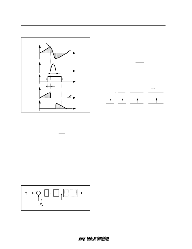
Figure49
High level duration (T10) of Pin 10 output signal
must be higher than the delay interval ”t
S(MAX)
” +
the flyback time (i.e. 8 + 12 = 20
μ
s) and must
turn-off beforethe end of diode conduction:
T
10
< t
S(Min.)
+ t
LF
+t
trace
2
< 40
μ
s
In practice,one will select the pin 1 capacitor
C1 = 3.3nF to yield T
10
= 29
μ
s.
V.5.3 - Characteristicsof loop ”
φ
2
”
The function to calculate is a time with respect to
the origintime setby”V
φ2
”. Infact,itis aneasytask
to inter-relatethe horizontaldisplacement (in mm)
to a time interval specified in
μ
s.
For a large screen widthof 540mm, the horizontal
scanning time : 64 - 12 = 52
μ
s, whichcorresponds
to :
≈
10mm/
μ
s.
B
Delay
d
t
)
t
IN
t
OUT
LF
Middle
of
Scanning
Flyback
V
2
V
i
t
t
OUT
t
IN
f(p)
A
2
Figure50
- i = A. (t
IN
- t
OUT
)(1)
- V = Z
i +Z
- t
OUT
- t
IN
= B
V + t
d
- 59.7
μ
s
R
K
V
CC
- Z
I
IN
(2)
(3)
- Z =
R
′
1
+ τ
p
- R’= R
IN
// R
- A= 17
μ
A/
μ
s
-
τ
= R’C
- B = 16.4
μ
s/V
The open-loop dynamic gain is :
T = ABf(p) = ABZ =ABR
′
1
+ τ
p
(4)
The system exhibits the characteristicsinherent to
a first ordercircuit and is therefore stable.
Combining equations(1), (2), (3) and (4), the t
OUT
delayis foundas follows :
It is thereforeclear that the second phase-locked
loop does not cause any dynamic delay.
This can be explained by the fact that the phase
modulatorresponds instanenouslyto allvariations
of ”
φ
2
”.
V.5.3.1 - Study of the Static Error
t
IN
= 0 (phase of V
φ2
) is taken as timingreference.
The equivalent impedance of F(p) filter is :
- R’= 460k
(R// R
IN
) : if an adjustmentis applied
to Pin16, or
- Modulatorinputresistance RIN = 25M
:without
adjustment
A. PHASE SHIFT ERROR IN CASE OF
NO ADJUSTMENT
Equation(5) becomes:
T
OUT
=BR
IN
I
IN
1
+
T
1
with: T1 = ABR
IN
Where :
- R
IN
= 25M
- I
IN
= 0.65mA
- t
d
= 10
μ
s
- T1 = 6.8
10
3
= 76dB
+t
D
59.7
μ
s
1
+
T
1
t
OUT
= - 46ns
which corresponds to a
picture shift of 0.46mm !
The error is quite negligible and thanks to rather
high open-loop gain, the display accuracy with
respectto thephasesetby”
φ
2
”,isverysatisfactory.
t
OUT
IN
= t
IN
BZI
1 + T
+
t
59.7
μ
s
1 + T
D
+
BZ
R
1 + T
KV
CC
Error term due
to phase shift
adjustment
(if applicable)
Error term
due to delay
Error term
due to the
input current
”I
IN
”
Dynamic
gain = 1
2
TEA2028 - TEA2029 APPLICATIONNOTE
25/46
相關(guān)PDF資料 |
PDF描述 |
|---|---|
| TEA2028 | APPLICATION NOTE |
| TEA2028B | SWITCH MODE POWER SUPPLY PRIMARY CIRCUIT |
| TEA2128 | SWITCH MODE POWER SUPPLY PRIMARY CIRCUIT |
| TEA2164S | SWITCH MODE POWER SUPPLY PRIMARY CIRCUIT |
| TEA2029C | COLOR TV SCANNING AND POWER SUPPLY PROCESSOR |
相關(guān)代理商/技術(shù)參數(shù) |
參數(shù)描述 |
|---|---|
| TEA2029 | 制造商:STMICROELECTRONICS 制造商全稱:STMicroelectronics 功能描述:APPLICATION NOTE |
| TEA2029C | 制造商:STMICROELECTRONICS 制造商全稱:STMicroelectronics 功能描述:COLOR TV SCANNING AND POWER SUPPLY PROCESSOR |
| TEA2029CV | 制造商:TEMIC 制造商全稱:TEMIC Semiconductors 功能描述:Timing Processor (LINE, FRAME, SMPS) for TV Sets |
| TEA2031A | 功能描述:視頻 IC East/West Correction RoHS:否 制造商:Fairchild Semiconductor 工作電源電壓:5 V 電源電流:80 mA 最大工作溫度:+ 85 C 封裝 / 箱體:TSSOP-28 封裝:Reel |
| TEA2031A_07 | 制造商:STMICROELECTRONICS 制造商全稱:STMicroelectronics 功能描述:COLOR TV EAST-WEST CORRECTION |
發(fā)布緊急采購,3分鐘左右您將得到回復(fù)。