- 您現(xiàn)在的位置:買(mǎi)賣(mài)IC網(wǎng) > PDF目錄98249 > TLV1571IPWLE (TEXAS INSTRUMENTS INC) 1-CH 10-BIT SUCCESSIVE APPROXIMATION ADC, PARALLEL ACCESS, PDSO24 PDF資料下載
參數(shù)資料
| 型號(hào): | TLV1571IPWLE |
| 廠商: | TEXAS INSTRUMENTS INC |
| 元件分類(lèi): | ADC |
| 英文描述: | 1-CH 10-BIT SUCCESSIVE APPROXIMATION ADC, PARALLEL ACCESS, PDSO24 |
| 文件頁(yè)數(shù): | 25/26頁(yè) |
| 文件大?。?/td> | 388K |
| 代理商: | TLV1571IPWLE |
第1頁(yè)第2頁(yè)第3頁(yè)第4頁(yè)第5頁(yè)第6頁(yè)第7頁(yè)第8頁(yè)第9頁(yè)第10頁(yè)第11頁(yè)第12頁(yè)第13頁(yè)第14頁(yè)第15頁(yè)第16頁(yè)第17頁(yè)第18頁(yè)第19頁(yè)第20頁(yè)第21頁(yè)第22頁(yè)第23頁(yè)第24頁(yè)當(dāng)前第25頁(yè)第26頁(yè)

TLV1571, TLV1578
2.7 V TO 5.5 V, 1-/8-CHANNEL, 10-BIT,
PARALLEL ANALOG-TO-DIGITAL CONVERTERS
SLAS170A –MARCH 1999 – REVISED AUGUST 1999
8
POST OFFICE BOX 655303
DALLAS, TEXAS 75265
detailed description (continued)
reference voltage input
The TLV1571/TLV1578 has two reference input pins: REFP and REFM. The voltage levels applied to these pins
establish the upper and lower limits of the analog inputs to produce a full-scale and zero-scale reading
respectively. The values of REFP, REFM, and the analog input should not exceed the positive supply or be less
than GND consistent with the specified absolute maximum ratings. The digital output is at full scale when the
input signal is equal to or higher than REFP and is at zero when the input signal is equal to or lower than REFM.
sampling/conversion
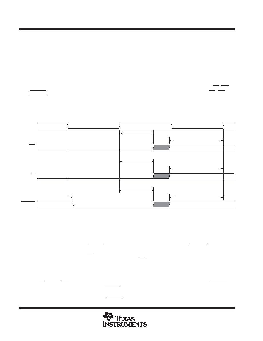
All sampling, conversion, and data output in the device are started by a trigger. This could be the RD, WR, or
CSTART signal depending on the mode of conversion and configuration. The rising edge of RD, WR, and
CSTART signal are extremely important, since they are used to start the conversion. These edges need to stay
close to the rising edge of the external clock (if they are used as CLK). The minimum setup and hold time with
respect to the rising edge of the external clock should be 5 ns minimum. When the internal clock is used, this
is not an issue since these two edges will start the internal clock automatically. Therefore, the setup time is
always met.
NOTE: tsu = setup time, th = hold time
ExtClk
WR
RD
CSTART
tsu(WRH_EXTCLKH) ≥5 ns
th(WRL_EXTCLKH) ≥5 ns
th(RDL_EXTCLKH) ≥5 ns
td(EXTCLK_CSTARTL) ≥5 ns
th(CSTARTL_EXTCLKH) ≥5 ns
tsu(CSTARTH_EXTCLKH)
≥5 ns
OR
tsu(RDH_EXTCLKH) ≥5 ns
Figure 3. Trigger Timing – Software Start Mode Using External Clock
start of conversion mechanism
There are two ways to convert data: hardware and software. In the hardware conversion mode the ADC begins
sampling at the falling edge of CSTART and begins conversion at the rising edge of CSTART. Software start
mode ADC samples for 6 clocks, then conversion occurs for ten clocks. The total sampling and conversion
process lasts only 16 clocks. If RD is not detected during the next clock cycle, the ADC automatically proceeds
to a power down state. Data is valid on the rising edge of INT in both conversion modes.
hardware CSTART conversion
external clock
With CS low and WR low, data is written into the ADC. The sampling begins at the falling edge of CSTART and
conversion begins at the rising edge of CSTART. At the end of conversion, EOC goes from low to high, telling
the host that conversion is ready to be read out. The external clock is active and is used as the reference at all
times. With this mode, it is required that CSTART is not applied at the rising edge of the clock (see Figure 4).
相關(guān)PDF資料 |
PDF描述 |
|---|---|
| TLV1571IDWRG4 | 1-CH 10-BIT SUCCESSIVE APPROXIMATION ADC, PARALLEL ACCESS, PDSO24 |
| TLV1571CDWRG4 | 1-CH 10-BIT SUCCESSIVE APPROXIMATION ADC, PARALLEL ACCESS, PDSO24 |
| TLV1572CD | 1-CH 10-BIT SUCCESSIVE APPROXIMATION ADC, SERIAL ACCESS, PDSO8 |
| TLV1572CDRG4 | 1-CH 10-BIT SUCCESSIVE APPROXIMATION ADC, SERIAL ACCESS, PDSO8 |
| TLV1572ID | 1-CH 10-BIT SUCCESSIVE APPROXIMATION ADC, SERIAL ACCESS, PDSO8 |
相關(guān)代理商/技術(shù)參數(shù) |
參數(shù)描述 |
|---|---|
| TLV1572 | 制造商:TI 制造商全稱(chēng):Texas Instruments 功能描述:2.7 V TO 5.5 V, 10-BIT, 1.25 MSPS SERIAL ANALOG-TO-DIGITAL CONVERTER WITH AUTO-POWERDOWN |
| TLV1572CD | 功能描述:模數(shù)轉(zhuǎn)換器 - ADC 10bit A/D RoHS:否 制造商:Texas Instruments 通道數(shù)量:2 結(jié)構(gòu):Sigma-Delta 轉(zhuǎn)換速率:125 SPs to 8 KSPs 分辨率:24 bit 輸入類(lèi)型:Differential 信噪比:107 dB 接口類(lèi)型:SPI 工作電源電壓:1.7 V to 3.6 V, 2.7 V to 5.25 V 最大工作溫度:+ 85 C 安裝風(fēng)格:SMD/SMT 封裝 / 箱體:VQFN-32 |
| TLV1572CDG4 | 功能描述:模數(shù)轉(zhuǎn)換器 - ADC 10-Bit 1.25 MSPS 1-Ch DSP RoHS:否 制造商:Texas Instruments 通道數(shù)量:2 結(jié)構(gòu):Sigma-Delta 轉(zhuǎn)換速率:125 SPs to 8 KSPs 分辨率:24 bit 輸入類(lèi)型:Differential 信噪比:107 dB 接口類(lèi)型:SPI 工作電源電壓:1.7 V to 3.6 V, 2.7 V to 5.25 V 最大工作溫度:+ 85 C 安裝風(fēng)格:SMD/SMT 封裝 / 箱體:VQFN-32 |
| TLV1572CDR | 功能描述:模數(shù)轉(zhuǎn)換器 - ADC 10-Bit 1.25 MSPS 1-Ch DSP RoHS:否 制造商:Texas Instruments 通道數(shù)量:2 結(jié)構(gòu):Sigma-Delta 轉(zhuǎn)換速率:125 SPs to 8 KSPs 分辨率:24 bit 輸入類(lèi)型:Differential 信噪比:107 dB 接口類(lèi)型:SPI 工作電源電壓:1.7 V to 3.6 V, 2.7 V to 5.25 V 最大工作溫度:+ 85 C 安裝風(fēng)格:SMD/SMT 封裝 / 箱體:VQFN-32 |
| TLV1572CDRG4 | 功能描述:模數(shù)轉(zhuǎn)換器 - ADC 10-Bit 1.25 MSPS 1-Ch DSP RoHS:否 制造商:Texas Instruments 通道數(shù)量:2 結(jié)構(gòu):Sigma-Delta 轉(zhuǎn)換速率:125 SPs to 8 KSPs 分辨率:24 bit 輸入類(lèi)型:Differential 信噪比:107 dB 接口類(lèi)型:SPI 工作電源電壓:1.7 V to 3.6 V, 2.7 V to 5.25 V 最大工作溫度:+ 85 C 安裝風(fēng)格:SMD/SMT 封裝 / 箱體:VQFN-32 |
發(fā)布緊急采購(gòu),3分鐘左右您將得到回復(fù)。