- 您現(xiàn)在的位置:買(mǎi)賣IC網(wǎng) > PDF目錄384014 > TMC2302A (Fairchild Semiconductor Corporation) Image Manipulation Sequencer PDF資料下載
參數(shù)資料
| 型號(hào): | TMC2302A |
| 廠商: | Fairchild Semiconductor Corporation |
| 英文描述: | Image Manipulation Sequencer |
| 中文描述: | 圖像處理序列 |
| 文件頁(yè)數(shù): | 8/36頁(yè) |
| 文件大小: | 188K |
| 代理商: | TMC2302A |
第1頁(yè)第2頁(yè)第3頁(yè)第4頁(yè)第5頁(yè)第6頁(yè)第7頁(yè)當(dāng)前第8頁(yè)第9頁(yè)第10頁(yè)第11頁(yè)第12頁(yè)第13頁(yè)第14頁(yè)第15頁(yè)第16頁(yè)第17頁(yè)第18頁(yè)第19頁(yè)第20頁(yè)第21頁(yè)第22頁(yè)第23頁(yè)第24頁(yè)第25頁(yè)第26頁(yè)第27頁(yè)第28頁(yè)第29頁(yè)第30頁(yè)第31頁(yè)第32頁(yè)第33頁(yè)第34頁(yè)第35頁(yè)第36頁(yè)
TMC2302A
PRODUCT SPECIFICATION
8
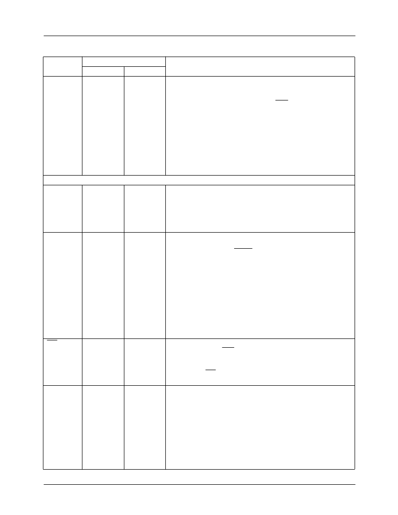
P
TADR
11-0
N12, N11,
M10, L9,
N10, M9,
N9, L8, M8,
N8, N7, M7
56, 55, 54,
53, 52, 51,
50, 49, 48,
47, 46, 44
Target Address.
the target image pixel value just resampled is output through the
Target Address Port TADR
11-0
. This port is forced into the high-
impedance state by the enable control OET. TADR
delayed up to seven clock cycles after the nominal sequence
shown in Table 4 by utilization of the pipeline delay parameter
PIPTAD. For systems requiring greater spatial resolution in the
source image than that offered by the SADR
Address Port can be reconfigured to output 12 additional LSBs of
the source address by placing the device into the Extended mode,
in which case the pipeline delay parameter must be set to 0 to
maintain alignment with the current source address port output.
See the Device Configuration and Control Parameters section.
The 12-bit address of one dimension (U, V, W) of
11-0
can be
23-0
alone, the Target
Controls
INIT
K12
67
Initialize.
the start of a new image transformation, and the internal working
registers are updated with the contents of the current control
parameter preload registers when the registered control input INIT
is HIGH. The image transformation then commences with the first
source image pixel address nine clocks after INIT is returned low.
Run/Halt.
The user can select between continuous or one-frame
operation with the registered input control SYNC. Assuming that
INIT remains LOW and NOOP remains HIGH, if SYNC remains
HIGH at the end of a transform the TMC2302A will begin the next
image transformation without interruption. This assumes either that
the user is not changing the parameter set, or that a new set of
parameters has already been loaded into the preload registers
midframe, prior to the beginning of the last line in the transform. If
SYNC is LOW during the last clock cycle of a transform, the device
will complete the image, having loaded the new transform
parameter set during the first clock of the final line of the transform,
and halt in the state set on the first clock cycle of the next
transform. These outputs are held until SYNC is again brought
HIGH, and operation resumes on the next clock. See Figure 5.
Input Parameter Chip Select.
The input parameter preload
register write clock IWR, and thus the preloading of all
configuration and transformation parameters, is disabled on the
next clock when the registered Input parameter Chip Select input is
HIGH. When ICS returns LOW, they are enabled on the next clock.
See Figure 3
.
Accumulate.
The external pixel interpolator or multiplier-
accumulator is initialized for a new accumulation of products by the
registered Accumulator Control output ACC. On the first cycle of
each interpolation walk, this output goes LOW for one cycle,
effectively clearing the register by loading in only the first new
resampled pixel value. When performing nearest-neighbor
resampling, this control will remain LOW throughout the entire
transform. This output can be delayed up to seven clock cycles
after the nominal sequence shown in Table 4 by the pipeline delay
parameter PIPACC. See the Device Configuration and Control
Parameters section.
The TMC2302A control logic is cleared and initialized for
SYNC
H13
74
ICS
B9
100
ACC
M1
27
Pin Descriptions
(continued)
Pin Name
Pin Number
PPGA
Pin Function Description
MQFP
相關(guān)PDF資料 |
PDF描述 |
|---|---|
| TMC2302AH5C | Image Manipulation Sequencer |
| TMC2302AH5C1 | Image Manipulation Sequencer |
| TMC2302AKEC | Image Manipulation Sequencer |
| TMC2302AKEC1 | Image Manipulation Sequencer |
| TMC2330AH5C | Coordinate Transformer 16 x 16 Bit, 40 MOPS |
相關(guān)代理商/技術(shù)參數(shù) |
參數(shù)描述 |
|---|---|
| TMC2302AH5C | 制造商:Rochester Electronics LLC 功能描述:- Bulk 制造商:Fairchild Semiconductor Corporation 功能描述: |
| TMC2302AH5C1 | 制造商:Rochester Electronics LLC 功能描述:- Bulk 制造商:Fairchild Semiconductor Corporation 功能描述: |
| TMC2302AKEC | 制造商:FAIRCHILD 制造商全稱:Fairchild Semiconductor 功能描述:Image Manipulation Sequencer |
| TMC2302AKEC1 | 制造商:FAIRCHILD 制造商全稱:Fairchild Semiconductor 功能描述:Image Manipulation Sequencer |
| TMC2330A | 制造商:CADEKA 制造商全稱:CADEKA 功能描述:Coordinate Transformer 16 x 16 Bit, 40 MOPS |
發(fā)布緊急采購(gòu),3分鐘左右您將得到回復(fù)。