- 您現(xiàn)在的位置:買賣IC網(wǎng) > PDF目錄368671 > TMS320C242FNA 16-Bit Digital Signal Processor PDF資料下載
參數(shù)資料
| 型號(hào): | TMS320C242FNA |
| 元件分類: | 數(shù)字信號(hào)處理 |
| 英文描述: | 16-Bit Digital Signal Processor |
| 中文描述: | 16位數(shù)字信號(hào)處理器 |
| 文件頁數(shù): | 44/66頁 |
| 文件大小: | 803K |
| 代理商: | TMS320C242FNA |
第1頁第2頁第3頁第4頁第5頁第6頁第7頁第8頁第9頁第10頁第11頁第12頁第13頁第14頁第15頁第16頁第17頁第18頁第19頁第20頁第21頁第22頁第23頁第24頁第25頁第26頁第27頁第28頁第29頁第30頁第31頁第32頁第33頁第34頁第35頁第36頁第37頁第38頁第39頁第40頁第41頁第42頁第43頁當(dāng)前第44頁第45頁第46頁第47頁第48頁第49頁第50頁第51頁第52頁第53頁第54頁第55頁第56頁第57頁第58頁第59頁第60頁第61頁第62頁第63頁第64頁第65頁第66頁
TMS320C242
DSP CONTROLLER
SPRS063B – DECEMBER 1997 – REVISED DECEMBER 1999
44
POST OFFICE BOX 1443
HOUSTON, TEXAS 77251–1443
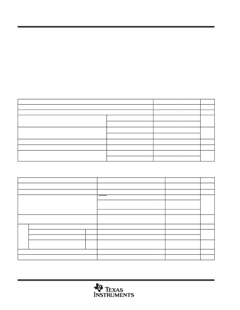
absolute maximum ratings over operating free-air temperature range (unless otherwise noted)
Supply voltage range, V
DD
. . . . . . . . . . . . . . . . . . . . . . . . . . . . . . . . . . . . . . . . . . . . . . . . . . . . . . . . .
Input voltage range
. . . . . . . . . . . . . . . . . . . . . . . . . . . . . . . . . . . . . . . . . . . . . . . . . . . . . . . . . . . . . . . . .
Output voltage range
. . . . . . . . . . . . . . . . . . . . . . . . . . . . . . . . . . . . . . . . . . . . . . . . . . . . . . . . . . . . . . .
Input clamp current I
IK
(V
I
< 0 or V
I
> V
DD
)
. . . . . . . . . . . . . . . . . . . . . . . . . . . . . . . . . . . . . . . . . . . . . . . . .
Output clamp current I
OK
(V
O
< 0 or V
O
> V
DD
)
. . . . . . . . . . . . . . . . . . . . . . . . . . . . . . . . . . . . . . . . . . . .
Operating free-air temperature range, T
A
: A version(’C242)
S version(’C242)
Storage temperature range, T
stg
. . . . . . . . . . . . . . . . . . . . . . . . . . . . . . . . . . . . . . . . . . . . . . . . . . . .
Stresses beyond those listed under “absolute maximum ratings” may cause permanent damage to the device. These are stress ratings only, and
functional operation of the device at these or any other conditions beyond those indicated under “recommended operating conditions” is not
implied. Exposure to absolute-maximum-rated conditions for extended periods may affect device reliability.
All voltage values are with respect to VSS.
recommended operating conditions
§
–0.3 V to 7 V
–0.3 V to 7 V
–0.3 V to 7 V
±
20 mA
±
20 mA
–40
°
C to 85
°
C
–40
°
C to 125
°
C
–55
°
C to 150
°
C
. . . . . . . . . . . . . . . . . . . . . . . . . . . .
. . . . . . . . . . . . . . . . . . . . . . . . . . .
MIN
NOM
MAX
UNIT
VDD
VSS
Supply voltage
4.5
5
5.5
V
Supply ground
0
V
XTAL1/CLKIN
3
VDD + 0.3
VDD + 0.3
+ 0 3
VIH
High level input voltage
High-level input voltage
V
All other inputs
2
XTAL1/CLKIN
0 3
–0.3
0 7
0.7
VIL
Low level input voltage
Low-level input voltage
V
All other inputs
–0.3
0.7
IOH
IOL
High-level output current VOH= 2 4 V
High-level output current, VOH = 2.4 V
Low-level output current VOL= 0 7 V
Low-level output current, VOL = 0.7 V
All outputs
–8
mA
All outputs
A version
8
mA
TA
Operating free air temperature
Operating free-air temperature
–40
85
°
C
S version
–40
125
§Thermal resistance values,
Θ
JA (junction-to-ambient) and
Θ
JC (junction-to-case) for the ’C242 can be found on the mechanical package pages.
electrical characteristics over recommended operating free-air temperature range (unless
otherwise noted)
PARAMETER
TEST CONDITIONS
MIN
TYP
MAX
UNIT
VOH
High-level output voltage
5-V operation, IOH = MAX = 8 mA
2.4
V
VOL
Low-level output voltage
5-V operation, IOL = MAX = 8 mA
TRST pins with internal pulldown
0.7
V
350
II
Input current (VI = VSS or VDD)
EMU0, EMU1, TMS, TCK, and TDI
with internal pullup (NMI, XF, BIO)
–350
65
μ
A
All other input-only pins
–5
5
IOZ
Output current, high-impedance state
(off-state)
VO = VDD or 0 V
–5
1
5
μ
A
Supply current, operating mode
5-V operation, tc(CO) = 50 ns
5-V operation, tc(CO) = 50 ns
5-V operation, tc(CO) = 50 ns
100
mA
Supply current, Idle 1 low-power mode
LPM0
40
mA
IDD#
Supply current, Idle 2 low-power mode
LPM1
35
Supply current, PLL/OSC power-down
mode
LPM2
5-V operation, at room temperature
75
μ
A
Ci
These three pins are pulled high only on the ’C242, not on emulation devices such as ’F243/’F241.
#In operating mode, the CPU is running a dummy code in B0 program memory. In all IDLE modes, the CPU is idle in B0 program memory.
Input capacitance
15
pF
Output capacitance
15
pF
A
相關(guān)PDF資料 |
PDF描述 |
|---|---|
| TMS320C241 | 16-Bit Digital Signal Processor |
| TMS320C242FNS | 16-Bit Digital Signal Processor |
| TMS320C242PGA | 16-Bit Digital Signal Processor |
| TMS320C242PGS | 16-Bit Digital Signal Processor |
| TMS320C30GEL | 32-Bit Digital Signal Processor |
相關(guān)代理商/技術(shù)參數(shù) |
參數(shù)描述 |
|---|---|
| TMS320C242FNS | 制造商:未知廠家 制造商全稱:未知廠家 功能描述:16-Bit Digital Signal Processor |
| TMS320C242PG | 制造商:TI 制造商全稱:Texas Instruments 功能描述:DSP CONTROLLER |
| TMS320C242PGA | 制造商:未知廠家 制造商全稱:未知廠家 功能描述:16-Bit Digital Signal Processor |
| TMS320C242PGS | 制造商:未知廠家 制造商全稱:未知廠家 功能描述:16-Bit Digital Signal Processor |
| TMS320C25 | 制造商:TI 制造商全稱:Texas Instruments 功能描述:SECOND-GENERATION DIGITAL SIGNAL PROCESSORS |
發(fā)布緊急采購,3分鐘左右您將得到回復(fù)。