- 您現(xiàn)在的位置:買(mǎi)賣(mài)IC網(wǎng) > PDF目錄300038 > TMS320LF2407APGEA (TEXAS INSTRUMENTS INC) 16-BIT, 20 MHz, OTHER DSP, PQFP144 PDF資料下載
參數(shù)資料
| 型號(hào): | TMS320LF2407APGEA |
| 廠商: | TEXAS INSTRUMENTS INC |
| 元件分類(lèi): | 數(shù)字信號(hào)處理 |
| 英文描述: | 16-BIT, 20 MHz, OTHER DSP, PQFP144 |
| 封裝: | GREEN, PLASTIC, LQFP-144 |
| 文件頁(yè)數(shù): | 43/134頁(yè) |
| 文件大小: | 1724K |
| 代理商: | TMS320LF2407APGEA |
第1頁(yè)第2頁(yè)第3頁(yè)第4頁(yè)第5頁(yè)第6頁(yè)第7頁(yè)第8頁(yè)第9頁(yè)第10頁(yè)第11頁(yè)第12頁(yè)第13頁(yè)第14頁(yè)第15頁(yè)第16頁(yè)第17頁(yè)第18頁(yè)第19頁(yè)第20頁(yè)第21頁(yè)第22頁(yè)第23頁(yè)第24頁(yè)第25頁(yè)第26頁(yè)第27頁(yè)第28頁(yè)第29頁(yè)第30頁(yè)第31頁(yè)第32頁(yè)第33頁(yè)第34頁(yè)第35頁(yè)第36頁(yè)第37頁(yè)第38頁(yè)第39頁(yè)第40頁(yè)第41頁(yè)第42頁(yè)當(dāng)前第43頁(yè)第44頁(yè)第45頁(yè)第46頁(yè)第47頁(yè)第48頁(yè)第49頁(yè)第50頁(yè)第51頁(yè)第52頁(yè)第53頁(yè)第54頁(yè)第55頁(yè)第56頁(yè)第57頁(yè)第58頁(yè)第59頁(yè)第60頁(yè)第61頁(yè)第62頁(yè)第63頁(yè)第64頁(yè)第65頁(yè)第66頁(yè)第67頁(yè)第68頁(yè)第69頁(yè)第70頁(yè)第71頁(yè)第72頁(yè)第73頁(yè)第74頁(yè)第75頁(yè)第76頁(yè)第77頁(yè)第78頁(yè)第79頁(yè)第80頁(yè)第81頁(yè)第82頁(yè)第83頁(yè)第84頁(yè)第85頁(yè)第86頁(yè)第87頁(yè)第88頁(yè)第89頁(yè)第90頁(yè)第91頁(yè)第92頁(yè)第93頁(yè)第94頁(yè)第95頁(yè)第96頁(yè)第97頁(yè)第98頁(yè)第99頁(yè)第100頁(yè)第101頁(yè)第102頁(yè)第103頁(yè)第104頁(yè)第105頁(yè)第106頁(yè)第107頁(yè)第108頁(yè)第109頁(yè)第110頁(yè)第111頁(yè)第112頁(yè)第113頁(yè)第114頁(yè)第115頁(yè)第116頁(yè)第117頁(yè)第118頁(yè)第119頁(yè)第120頁(yè)第121頁(yè)第122頁(yè)第123頁(yè)第124頁(yè)第125頁(yè)第126頁(yè)第127頁(yè)第128頁(yè)第129頁(yè)第130頁(yè)第131頁(yè)第132頁(yè)第133頁(yè)第134頁(yè)
TMS320LF2407A,TMS320LF2406A,TMS320LF2403A,TMS320LF2402A
TMS320LC2406A,TMS320LC2404A,TMS320LC2403A,TMS320LC2402A
DSP CONTROLLERS
SPRS145L JULY 2000 REVISED SEPTEMBER 2007
16
POST OFFICE BOX 1443
HOUSTON, TEXAS 772511443
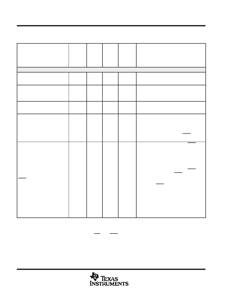
pin functions (continued)
Table 2. LF240xA and LC240xA Pin List and Package Options (Continued)
PIN NAME
LF2407A
(144-PGE)
2406A
(100-PZ)
LC2404A
(100-PZ)
2403A,
LC2402A
(64-PAG)
and
2402A
(64-PG)
DESCRIPTION
EMULATION AND TEST (CONTINUED)
TDI
139
96
30
JTAG test data input (TDI) with internal pullup. TDI
is clocked into the selected register (instruction or
data) on a rising edge of TCK.
(
↑)
TDO
142
99
31
JTAG scan out, test data output (TDO). The
contents of the selected register (instruction or
data) is shifted out of TDO on the falling edge of
TCK.
(
↓)
TMS
144
100
32
JTAG test-mode select (TMS) with internal pullup.
This serial control input is clocked into the TAP
controller on the rising edge of TCK.
(
↑)
TMS2
36
25
48
JTAG test-mode select 2 (TMS2) with internal
pullup. This serial control input is clocked into the
TAP controller on the rising edge of TCK. Used for
test and emulation only. This pin can be left
unconnected in user applications. If the PLL bypass
mode is desired, TMS2, TMS, and TRST should be
held low during reset.
(
↑)
TRST
1
33
JTAG test reset with internal pulldown. TRST, when
driven high, gives the scan system control of the
operations of the device. If this signal is not
connected or driven low, the device operates in its
functional mode, and the test reset signals are
ignored.
(
↓)
NOTE: Do not use pullup resistors on TRST; it has
an internal pulldown device. TRST is an active high
test pin and must be maintained low at all times
during normal device operation. In a low-noise
environment, TRST may be left floating. In other
instances, an external pulldown resistor is highly
recommended. The value of this resistor should be
based on drive strength of the debugger pods
applicable to the design. A 2.2-k
resistor generally
offers
adequate
protection.
Since
this
is
applicationspecific, it is recommended that each
target board be validated for proper operation of the
debugger and the application. (I
↓)
Bold, italicized pin names indicate pin function after reset.
GPIO General-purpose input/output pin. All GPIOs come up as input after reset.
§ It is highly recommended that VCCA be isolated from the digital supply voltage (and VSSA from digital ground) to maintain the specified accuracy
and improve the noise immunity of the ADC.
Only when all of the following conditions are met: EMU1/OFF is low, TRST is low, and EMU0 is high
# No power supply pin (VDD, VDDO, VCCA, VSS, or VSSO) should be left unconnected. All power supply pins must be connected appropriately for
proper device operation.
LEGEND:
↑ Internal pullup
↓ Internal pulldown
(Typical active pullup/pulldown value is
±16 A.)
相關(guān)PDF資料 |
PDF描述 |
|---|---|
| TMS426409AP-60DJ | 4M X 4 EDO DRAM, 60 ns, PDSO24 |
| TMS426809AP-70DGC | 2M X 8 EDO DRAM, 70 ns, PDSO28 |
| TMS44400DJ-80 | 1M X 4 FAST PAGE DRAM, 80 ns, PDSO20 |
| TMS470R1B768PGEQR | 32-BIT, FLASH, 60 MHz, RISC MICROCONTROLLER, PQFP144 |
| TMS4C1050-4DJL | 256K X 4 OTHER FIFO, PDSO20 |
相關(guān)代理商/技術(shù)參數(shù) |
參數(shù)描述 |
|---|---|
| TMS320LF2407APGEA | 制造商:Texas Instruments 功能描述:16BIT DSP FLASH SMD 320LF2407 |
| TMS320LF2407APGEG4 | 功能描述:數(shù)字信號(hào)處理器和控制器 - DSP, DSC 16-Bit Fixed-Pt DSP with Flash RoHS:否 制造商:Microchip Technology 核心:dsPIC 數(shù)據(jù)總線寬度:16 bit 程序存儲(chǔ)器大小:16 KB 數(shù)據(jù) RAM 大小:2 KB 最大時(shí)鐘頻率:40 MHz 可編程輸入/輸出端數(shù)量:35 定時(shí)器數(shù)量:3 設(shè)備每秒兆指令數(shù):50 MIPs 工作電源電壓:3.3 V 最大工作溫度:+ 85 C 封裝 / 箱體:TQFP-44 安裝風(fēng)格:SMD/SMT |
| TMS320LF2407APGES | 功能描述:數(shù)字信號(hào)處理器和控制器 - DSP, DSC 16-Bit Univ Bus Drv With 3-State Outputs RoHS:否 制造商:Microchip Technology 核心:dsPIC 數(shù)據(jù)總線寬度:16 bit 程序存儲(chǔ)器大小:16 KB 數(shù)據(jù) RAM 大小:2 KB 最大時(shí)鐘頻率:40 MHz 可編程輸入/輸出端數(shù)量:35 定時(shí)器數(shù)量:3 設(shè)備每秒兆指令數(shù):50 MIPs 工作電源電壓:3.3 V 最大工作溫度:+ 85 C 封裝 / 箱體:TQFP-44 安裝風(fēng)格:SMD/SMT |
| TMS320LF2407PGES | 制造商:Rochester Electronics LLC 功能描述:- Bulk |
| TMS320M640AGNZ4 | 制造商:Texas Instruments 功能描述:TMS320DM640 548PIN FCBGA PG2.0 - Trays |
發(fā)布緊急采購(gòu),3分鐘左右您將得到回復(fù)。