- 您現(xiàn)在的位置:買賣IC網(wǎng) > PDF目錄98282 > TPS54160DRCT (TEXAS INSTRUMENTS INC) SWITCHING REGULATOR, 2500 kHz SWITCHING FREQ-MAX, PDSO10 PDF資料下載
參數(shù)資料
| 型號(hào): | TPS54160DRCT |
| 廠商: | TEXAS INSTRUMENTS INC |
| 元件分類: | 穩(wěn)壓器 |
| 英文描述: | SWITCHING REGULATOR, 2500 kHz SWITCHING FREQ-MAX, PDSO10 |
| 封裝: | PLASTIC, SON-10 |
| 文件頁數(shù): | 13/50頁 |
| 文件大?。?/td> | 1375K |
| 代理商: | TPS54160DRCT |
第1頁第2頁第3頁第4頁第5頁第6頁第7頁第8頁第9頁第10頁第11頁第12頁當(dāng)前第13頁第14頁第15頁第16頁第17頁第18頁第19頁第20頁第21頁第22頁第23頁第24頁第25頁第26頁第27頁第28頁第29頁第30頁第31頁第32頁第33頁第34頁第35頁第36頁第37頁第38頁第39頁第40頁第41頁第42頁第43頁第44頁第45頁第46頁第47頁第48頁第49頁第50頁

( )
(
)
W =
RT
1.0888
SW
206033
R
k
f
kHz
0
100
200
300
400
500
200
300
400
500
600
700
800
900
1000
1100
RT/CLK-Resistance-kW
f
-SwitchingFrequency-kHz
s
1200
V =12V,
T =25°C
I
J
0
500
1000
1500
2000
2500
0
25
50
75
100
125
150
175
200
f
-SwitchingFrequency-kHz
s
RT/CLK-ClockResistance-kW
V =12V,
T =25°C
I
J
SLVS795C – OCTOBER 2008 – REVISED OCTOBER 2010
www.ti.com
DETAILED DESCRIPTION (continued)
Constant Switching Frequency and Timing Resistor (RT/CLK Pin)
The switching frequency of the TPS54160 is adjustable over a wide range from approximately 100kHz to
2500kHz by placing a resistor on the RT/CLK pin. The RT/CLK pin voltage is typically 0.5V and must have a
resistor to ground to set the switching frequency. To determine the timing resistance for a given switching
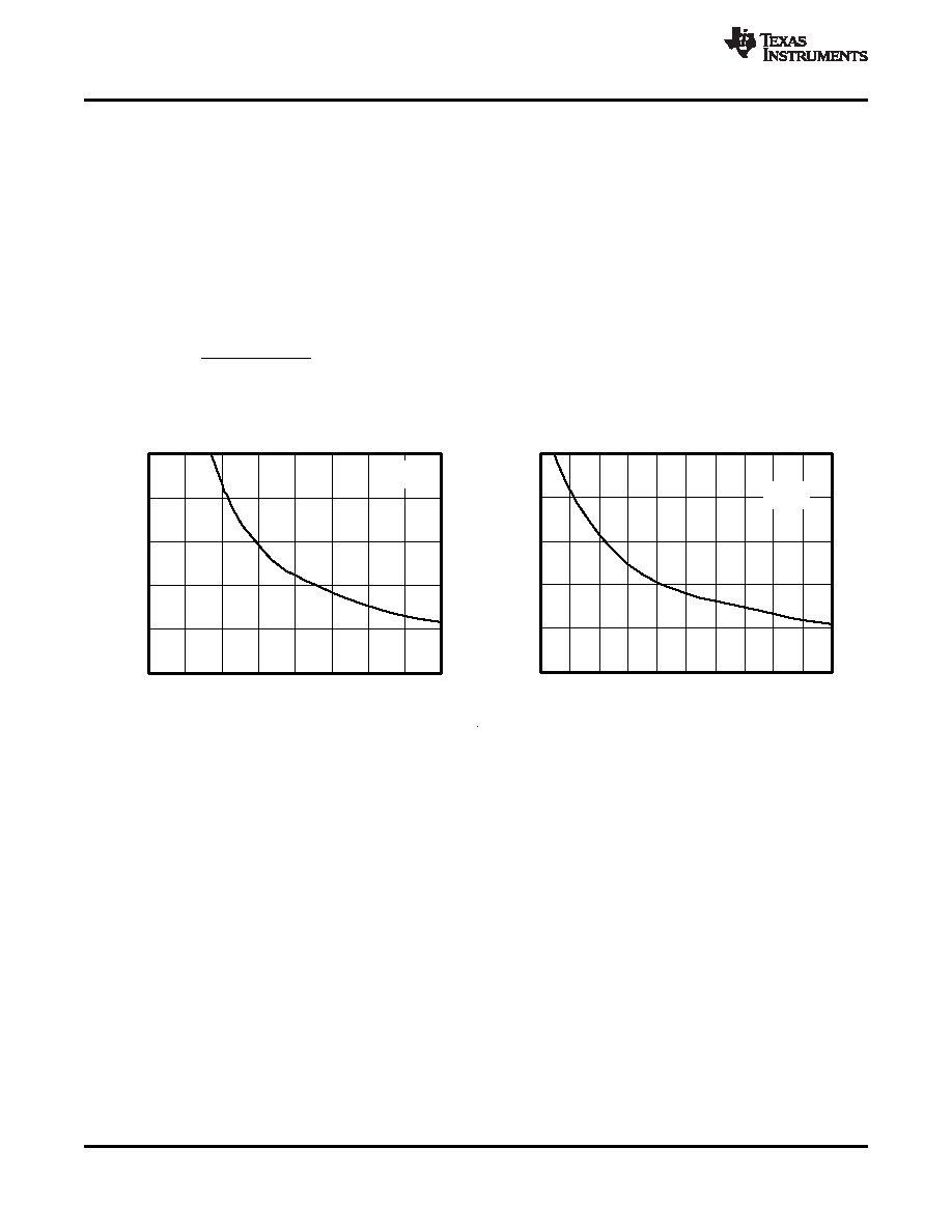
frequency, use Equation 11 or the curves in Figure 40 or Figure 41. To reduce the solution size one would
typically set the switching frequency as high as possible, but tradeoffs of the supply efficiency, maximum input
voltage and minimum controllable on time should be considered.
The minimum controllable on time is typically 130ns and limits the maximum operating input voltage.
The maximum switching frequency is also limited by the frequency shift circuit. More discussion on the details of
the maximum switching frequency is located below.
(11)
SWITCHING FREQUENCY
vs
RT/CLK RESISTANCE HIGH FREQUENCY RANGE
RT/CLK RESISTANCE LOW FREQUENCY RANGE
Figure 40. High Range Timing Resistance
Figure 41. Low Range RT
Overcurrent Protection and Frequency Shift
The TPS54160 implements current mode control which uses the COMP pin voltage to turn off the high-side
MOSFET on a cycle by cycle basis. Each cycle the switch current and COMP pin voltage are compared, when
the peak switch current intersects the COMP voltage, the high-side switch is turned off. During overcurrent
conditions that pull the output voltage low, the error amplifier responds by driving the COMP pin high, increasing
the switch current. The error amplifier output is clamped internally, which functions as a switch current limit.
To increase the maximum operating switching frequency at high input voltages the TPS54160 implements a
frequency shift. The switching frequency is divided by 8, 4, 2, and 1 as the voltage ramps from 0 to 0.8 volts on
VSENSE pin.
The device implements a digital frequency shift to enable synchronizing to an external clock during normal
startup and fault conditions. Since the device can only divide the switching frequency by 8, there is a maximum
input voltage limit in which the device operates and still have frequency shift protection.
During short-circuit events (particularly with high input voltage applications), the control loop has a finite minimum
controllable on time and the output has a low voltage. During the switch on time, the inductor current ramps to
the peak current limit because of the high input voltage and minimum on time. During the switch off time, the
inductor would normally not have enough off time and output voltage for the inductor to ramp down by the ramp
up amount. The frequency shift effectively increases the off time allowing the current to ramp down.
20
Copyright 2008–2010, Texas Instruments Incorporated
Product Folder Link(s): TPS54160
相關(guān)PDF資料 |
PDF描述 |
|---|---|
| TPS54160DGQ | 2.7 A SWITCHING REGULATOR, 2500 kHz SWITCHING FREQ-MAX, PDSO10 |
| TPS54160DGQR | 2.7 A SWITCHING REGULATOR, 2500 kHz SWITCHING FREQ-MAX, PDSO10 |
| TPS5420MDREPG4 | 5.2 A SWITCHING REGULATOR, 600 kHz SWITCHING FREQ-MAX, PDSO8 |
| TPS5420MDREP | 5.2 A SWITCHING REGULATOR, 600 kHz SWITCHING FREQ-MAX, PDSO8 |
| TPS54225PWP | 4.5 A SWITCHING REGULATOR, 700 kHz SWITCHING FREQ-MAX, PDSO14 |
相關(guān)代理商/技術(shù)參數(shù) |
參數(shù)描述 |
|---|---|
| TPS54160EVM-230 | 功能描述:電源管理IC開發(fā)工具 TPS54160 Eval Mod RoHS:否 制造商:Maxim Integrated 產(chǎn)品:Evaluation Kits 類型:Battery Management 工具用于評估:MAX17710GB 輸入電壓: 輸出電壓:1.8 V |
| TPS54160EVM-535 | 功能描述:電源管理IC開發(fā)工具 Eval Mod for High Brightness LED Drvr RoHS:否 制造商:Maxim Integrated 產(chǎn)品:Evaluation Kits 類型:Battery Management 工具用于評估:MAX17710GB 輸入電壓: 輸出電壓:1.8 V |
| TPS54160-Q1 | 制造商:TI 制造商全稱:Texas Instruments 功能描述:1.5-A 60-V STEP-DOWN SWIFT DC/DC CONVERTER WITH Eco-Mode CONTROL |
| TPS54160QDGQRDL | 制造商:Texas Instruments 功能描述:- Tape and Reel |
| TPS54160QDGQRQ1 | 功能描述:直流/直流開關(guān)調(diào)節(jié)器 Aut Cat 3.5-60V 1.5A Step Down Converter RoHS:否 制造商:International Rectifier 最大輸入電壓:21 V 開關(guān)頻率:1.5 MHz 輸出電壓:0.5 V to 0.86 V 輸出電流:4 A 輸出端數(shù)量: 最大工作溫度: 安裝風(fēng)格:SMD/SMT 封裝 / 箱體:PQFN 4 x 5 |
發(fā)布緊急采購,3分鐘左右您將得到回復(fù)。