- 您現(xiàn)在的位置:買賣IC網(wǎng) > PDF目錄98282 > TPS54160DRCT (TEXAS INSTRUMENTS INC) SWITCHING REGULATOR, 2500 kHz SWITCHING FREQ-MAX, PDSO10 PDF資料下載
參數(shù)資料
| 型號(hào): | TPS54160DRCT |
| 廠商: | TEXAS INSTRUMENTS INC |
| 元件分類: | 穩(wěn)壓器 |
| 英文描述: | SWITCHING REGULATOR, 2500 kHz SWITCHING FREQ-MAX, PDSO10 |
| 封裝: | PLASTIC, SON-10 |
| 文件頁(yè)數(shù): | 4/50頁(yè) |
| 文件大?。?/td> | 1375K |
| 代理商: | TPS54160DRCT |
第1頁(yè)第2頁(yè)第3頁(yè)當(dāng)前第4頁(yè)第5頁(yè)第6頁(yè)第7頁(yè)第8頁(yè)第9頁(yè)第10頁(yè)第11頁(yè)第12頁(yè)第13頁(yè)第14頁(yè)第15頁(yè)第16頁(yè)第17頁(yè)第18頁(yè)第19頁(yè)第20頁(yè)第21頁(yè)第22頁(yè)第23頁(yè)第24頁(yè)第25頁(yè)第26頁(yè)第27頁(yè)第28頁(yè)第29頁(yè)第30頁(yè)第31頁(yè)第32頁(yè)第33頁(yè)第34頁(yè)第35頁(yè)第36頁(yè)第37頁(yè)第38頁(yè)第39頁(yè)第40頁(yè)第41頁(yè)第42頁(yè)第43頁(yè)第44頁(yè)第45頁(yè)第46頁(yè)第47頁(yè)第48頁(yè)第49頁(yè)第50頁(yè)

VOUT
(ac)
I
L
PH
SLVS795C – OCTOBER 2008 – REVISED OCTOBER 2010
www.ti.com
DETAILED DESCRIPTION
Fixed Frequency PWM Control
The TPS54160 uses an adjustable fixed frequency, peak current mode control. The output voltage is compared
through external resistors on the VSENSE pin to an internal voltage reference by an error amplifier which drives
the COMP pin. An internal oscillator initiates the turn on of the high-side power switch. The error amplifier output
is compared to the high-side power switch current. When the power switch current reaches the level set by the
COMP voltage, the power switch is turned off. The COMP pin voltage will increase and decrease as the output
current increases and decreases. The device implements a current limit by clamping the COMP pin voltage to a
maximum level. The Eco-Mode is implemented with a minimum clamp on the COMP pin.
Slope Compensation Output Current
The TPS54160 adds a compensating ramp to the switch current signal. This slope compensation prevents
sub-harmonic oscillations. The available peak inductor current remains constant over the full duty cycle range.
Pulse Skip Eco-Mode
The TPS54160 operates in a pulse skip Eco mode at light load currents to improve efficiency by reducing
switching and gate drive losses. The TPS54160 is designed so that if the output voltage is within regulation and
the peak switch current at the end of any switching cycle is below the pulse skipping current threshold, the
device enters Eco mode. This current threshold is the current level corresponding to a nominal COMP voltage or
500mV.
When in Eco-mode, the COMP pin voltage is clamped at 500mV and the high-side MOSFET is inhibited. Further
decreases in load current or in output voltage can not drive the COMP pin below this clamp voltage level.
Since the device is not switching, the output voltage begins to decay. As the voltage control loop compensates
for the falling output voltage, the COMP pin voltage begins to rise. At this time, the high-side MOSFET is enabled
and a switching pulse initiates on the next switching cycle. The peak current is set by the COMP pin voltage. The
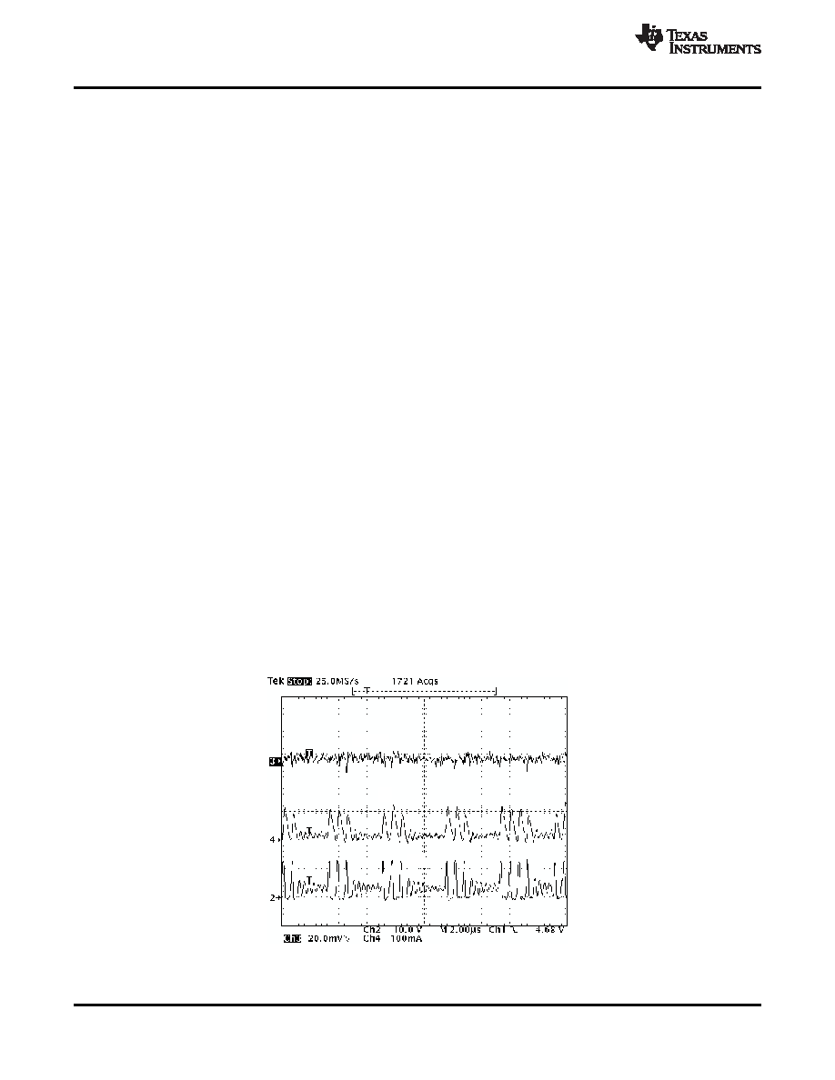
output voltage re-charges the regulated value (see Figure 25), then the peak switch current starts to decrease,
and eventually falls below the Eco mode threshold at which time the device again enters Eco mode.
For Eco mode operation, the TPS54160 senses peak current, not average or load current, so the load current
where the device enters Eco mode is dependent on the output inductor value. For example, the circuit in
Figure 51 enters Eco mode at about 18mA of output current. When the load current is low and the output voltage
is within regulation, the device enters a sleep mod,e and draws only 116mA input quiescent current. The internal
PLL remains operating when in sleep mode. When operating at light load currents in the pulse skip mode, the
switching transitions occur synchronously with the external clock signal.
Figure 25. Pulse Skip Mode Operation
12
Copyright 2008–2010, Texas Instruments Incorporated
Product Folder Link(s): TPS54160
相關(guān)PDF資料 |
PDF描述 |
|---|---|
| TPS54160DGQ | 2.7 A SWITCHING REGULATOR, 2500 kHz SWITCHING FREQ-MAX, PDSO10 |
| TPS54160DGQR | 2.7 A SWITCHING REGULATOR, 2500 kHz SWITCHING FREQ-MAX, PDSO10 |
| TPS5420MDREPG4 | 5.2 A SWITCHING REGULATOR, 600 kHz SWITCHING FREQ-MAX, PDSO8 |
| TPS5420MDREP | 5.2 A SWITCHING REGULATOR, 600 kHz SWITCHING FREQ-MAX, PDSO8 |
| TPS54225PWP | 4.5 A SWITCHING REGULATOR, 700 kHz SWITCHING FREQ-MAX, PDSO14 |
相關(guān)代理商/技術(shù)參數(shù) |
參數(shù)描述 |
|---|---|
| TPS54160EVM-230 | 功能描述:電源管理IC開發(fā)工具 TPS54160 Eval Mod RoHS:否 制造商:Maxim Integrated 產(chǎn)品:Evaluation Kits 類型:Battery Management 工具用于評(píng)估:MAX17710GB 輸入電壓: 輸出電壓:1.8 V |
| TPS54160EVM-535 | 功能描述:電源管理IC開發(fā)工具 Eval Mod for High Brightness LED Drvr RoHS:否 制造商:Maxim Integrated 產(chǎn)品:Evaluation Kits 類型:Battery Management 工具用于評(píng)估:MAX17710GB 輸入電壓: 輸出電壓:1.8 V |
| TPS54160-Q1 | 制造商:TI 制造商全稱:Texas Instruments 功能描述:1.5-A 60-V STEP-DOWN SWIFT DC/DC CONVERTER WITH Eco-Mode CONTROL |
| TPS54160QDGQRDL | 制造商:Texas Instruments 功能描述:- Tape and Reel |
| TPS54160QDGQRQ1 | 功能描述:直流/直流開關(guān)調(diào)節(jié)器 Aut Cat 3.5-60V 1.5A Step Down Converter RoHS:否 制造商:International Rectifier 最大輸入電壓:21 V 開關(guān)頻率:1.5 MHz 輸出電壓:0.5 V to 0.86 V 輸出電流:4 A 輸出端數(shù)量: 最大工作溫度: 安裝風(fēng)格:SMD/SMT 封裝 / 箱體:PQFN 4 x 5 |
發(fā)布緊急采購(gòu),3分鐘左右您將得到回復(fù)。