- 您現(xiàn)在的位置:買賣IC網(wǎng) > PDF目錄365969 > TSC21020F-20MBP833 IC CYCLONE III FPGA 25K 144-EQFP PDF資料下載
參數(shù)資料
| 型號: | TSC21020F-20MBP833 |
| 英文描述: | IC CYCLONE III FPGA 25K 144-EQFP |
| 中文描述: | 數(shù)字信號處理器| 32位|的CMOS | RAD數(shù)據(jù)通信硬| QFL | 256PIN |陶瓷 |
| 文件頁數(shù): | 9/51頁 |
| 文件大?。?/td> | 763K |
| 代理商: | TSC21020F-20MBP833 |
第1頁第2頁第3頁第4頁第5頁第6頁第7頁第8頁當(dāng)前第9頁第10頁第11頁第12頁第13頁第14頁第15頁第16頁第17頁第18頁第19頁第20頁第21頁第22頁第23頁第24頁第25頁第26頁第27頁第28頁第29頁第30頁第31頁第32頁第33頁第34頁第35頁第36頁第37頁第38頁第39頁第40頁第41頁第42頁第43頁第44頁第45頁第46頁第47頁第48頁第49頁第50頁第51頁

9
TSC21020F
4153F
–
AERO
–
06/03
System Interface
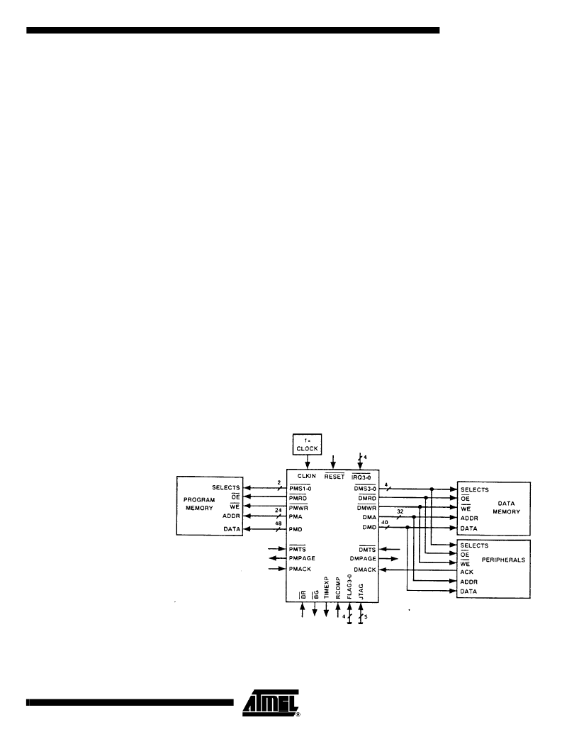
Figure 2 shows an TSC21020F basic system configuration.
The external memory interface supports memory- mapped peripherals and slower mem-
ory with a user-defined combination of programmable wait states and hardware
acknowledge signals. Both the program memory and data memory interfaces support
addressing of page-mode DRAMs.
The TSC21020F
’
s internal functions are supported by four internal buses: the program
memory address (PMA) and data memory address (DMA) buses are used for
addresses associated with program and data memory. The program memory data
(PMD) and data memory data (DMD) buses are used for data associated with the two
memory spaces. These buses are extended off chip. Four data memory select (DMS)
signals select one of four user-configurable banks of data memory. Similarly, two pro-
gram memory select (PMS) signals select between two user-configurable banks of
program memory. All banks are independently programmable for 0-7 wait states.
The PX registers permit passing data between program memory and data memory
spaces. They provide a bridge between the 48-bit PMD bus and the 40-bit DMD bus or
between the 40-bit register file and the PMD bus.
The PMA bus is 24 bits wide allowing direct access of up to 16M words of mixed instruc-
tion code and data. The PMD is 48 bits wide to accommodate the 48-bit instruction
width. For access of 40-bit data the lower 8 bits are unused. For access of 32-bit data
the lower 16 bits are ignored.
The DMA bus is 32 bits wide allowing direct access of up to 4 Gigawords of data. The
DMD bus is 40 bits wide. For 32-bit data, the lower 8 bits are unused. The DMD bus pro-
vides a path for the contents of any register in the processor to be transferred to any
other register or to any external data memory location in a single cycle. The data mem-
ory address comes from one of two sources: an absolute value specified in the
instruction code (direct addressing) or the output of a data address generator (indirect
addressing).
Figure 2.
Basic System Configuration
External devices can gain control of the processor
’
s memory buses from the
TSC21020F by means of the bus request/grant signals (BR and BG). To grant its buses
in response to a bus request, the TSC21020F halts internal operations and places its
相關(guān)PDF資料 |
PDF描述 |
|---|---|
| TSC21020F-20MBSB | IC CYCLONE III FPGA 25K 144 EQFP |
| TSC21020F-20MBSC | IC CYCLONE III FPGA 25K 256 FBGA |
| TSC21020F-20MBSL1 | IC CYCLONE III FPGA 25K 324 FBGA |
| TSC21020F-20MBSL2 | IC CYCLONE III FPGA 25K 324-FBGA |
| TSC427CPA-2 | IC FLEX 8000A FPGA 4K 84-PLCC |
相關(guān)代理商/技術(shù)參數(shù) |
參數(shù)描述 |
|---|---|
| TSC21020F-20MBSB | 制造商:未知廠家 制造商全稱:未知廠家 功能描述:DSP|32-BIT|CMOS| RAD HARD|QFL|256PIN|CERAMIC |
| TSC21020F-20MBSC | 制造商:未知廠家 制造商全稱:未知廠家 功能描述:DSP|32-BIT|CMOS| RAD HARD|QFL|256PIN|CERAMIC |
| TSC21020F-20MBSL1 | 制造商:未知廠家 制造商全稱:未知廠家 功能描述:DSP|32-BIT|CMOS| RAD HARD|QFL|256PIN|CERAMIC |
| TSC21020F-20MBSL2 | 制造商:未知廠家 制造商全稱:未知廠家 功能描述:DSP|32-BIT|CMOS| RAD HARD|QFL|256PIN|CERAMIC |
| TSC21020F-20MBSL3 | 制造商:未知廠家 制造商全稱:未知廠家 功能描述:DSP|32-BIT|CMOS| RAD HARD|QFL|256PIN|CERAMIC |
發(fā)布緊急采購,3分鐘左右您將得到回復(fù)。