- 您現(xiàn)在的位置:買賣IC網(wǎng) > PDF目錄98302 > TSC2117IRGZT (TEXAS INSTRUMENTS INC) SPECIALTY CONSUMER CIRCUIT, QCC48 PDF資料下載
參數(shù)資料
| 型號: | TSC2117IRGZT |
| 廠商: | TEXAS INSTRUMENTS INC |
| 元件分類: | 消費(fèi)家電 |
| 英文描述: | SPECIALTY CONSUMER CIRCUIT, QCC48 |
| 封裝: | 7 X 7 MM, GREEN, PLASTIC, VQFN-48 |
| 文件頁數(shù): | 45/192頁 |
| 文件大小: | 2728K |
| 代理商: | TSC2117IRGZT |
第1頁第2頁第3頁第4頁第5頁第6頁第7頁第8頁第9頁第10頁第11頁第12頁第13頁第14頁第15頁第16頁第17頁第18頁第19頁第20頁第21頁第22頁第23頁第24頁第25頁第26頁第27頁第28頁第29頁第30頁第31頁第32頁第33頁第34頁第35頁第36頁第37頁第38頁第39頁第40頁第41頁第42頁第43頁第44頁當(dāng)前第45頁第46頁第47頁第48頁第49頁第50頁第51頁第52頁第53頁第54頁第55頁第56頁第57頁第58頁第59頁第60頁第61頁第62頁第63頁第64頁第65頁第66頁第67頁第68頁第69頁第70頁第71頁第72頁第73頁第74頁第75頁第76頁第77頁第78頁第79頁第80頁第81頁第82頁第83頁第84頁第85頁第86頁第87頁第88頁第89頁第90頁第91頁第92頁第93頁第94頁第95頁第96頁第97頁第98頁第99頁第100頁第101頁第102頁第103頁第104頁第105頁第106頁第107頁第108頁第109頁第110頁第111頁第112頁第113頁第114頁第115頁第116頁第117頁第118頁第119頁第120頁第121頁第122頁第123頁第124頁第125頁第126頁第127頁第128頁第129頁第130頁第131頁第132頁第133頁第134頁第135頁第136頁第137頁第138頁第139頁第140頁第141頁第142頁第143頁第144頁第145頁第146頁第147頁第148頁第149頁第150頁第151頁第152頁第153頁第154頁第155頁第156頁第157頁第158頁第159頁第160頁第161頁第162頁第163頁第164頁第165頁第166頁第167頁第168頁第169頁第170頁第171頁第172頁第173頁第174頁第175頁第176頁第177頁第178頁第179頁第180頁第181頁第182頁第183頁第184頁第185頁第186頁第187頁第188頁第189頁第190頁第191頁第192頁
TSC2117
Low-Power Audio Codec With Embedded miniDSP, Stereo Class-D
Speaker Amplifier, and Smart Four-Wire Touch-Screen Controller
www.ti.com
SLAS550A – APRIL 2009 – REVISED JUNE 2009
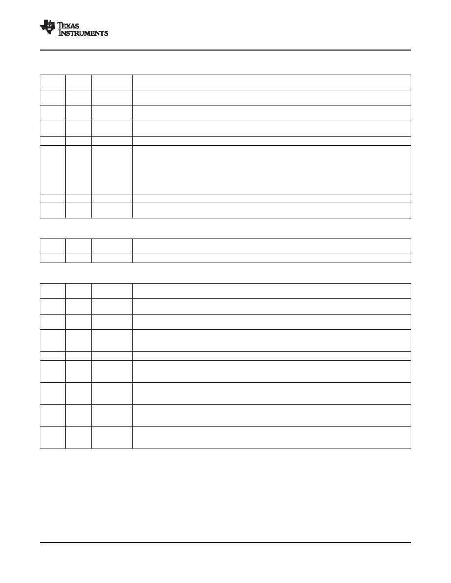
Page 3/Register 6: Voltage Reference
READ/
RESET
BIT
DESCRIPTION
WRITE
VALUE
D7
R/W
0
0: External reference is used for non-touch-screen measurement.
1: Internal reference is used for non-touch-screen measurement.
D6
R/W
0
0: Internal reference = 1.25 V
1: Internal reference = 2.5 V
D5
R/W
1
0: Internal reference powered up continuously for conversions
1: Internal reference powered up/down automatically based on whether conversion is in progress.
D4
R/W
0
Reserved
D3–D2
R/W
00
Reference Stabilization Time Before Conversion
00: 0
s
01: 100
s
10: 500
s
11: 1 ms
Note: These values are based on MCLK/DIV (page 3/register 17) = 8 MHz. Scale according to the
actual oscillator frequency.
D1
R/W
0
Reserved
D0
R/W
0
0: VBAT is the normal auxillary input (VBAT
≤ VREF).
1: VBAT = BAT is the battery input for battery measurement.
Page 3/Registers 7 to 8: Reserved
READ/
RESET
BIT
DESCRIPTION
WRITE
VALUE
D7–D0
R/W
XXXX XXXX
Reserved. Write only the reset value to these bits.
Page 3/Register 9: Status Bit
READ/
RESET
BIT
Description
WRITE
VALUE
D7
R
0
0: Pen touch is not detected.
1: Pen touch is detected.
D6
R
1
0: ADC is busy.
1: ADC is not busy.
D5
R
0
0: No new data is available.
1: New data is available. (This bit is cleared only after all the converted data have been completely read
out. This bit is not valid for the buffer mode.)
D4
R/W
X
Reserved. Write only the reset value to this bit.
D3
R
0
0: No new X data is available.
1: New data for X coordinate is available. (This bit is cleared only after the converted X data have been
read out. This bit is not valid for the buffer mode.)
D2
R
0
0: No new Y data is available.
1: New data for Y coordinate is available. (This bit is cleared only after the converted Y data have been
read out. This bit is not valid for the buffer mode.)
D1
R
0
0: No new Z1 data is available.
1: New data for Z1 coordinate is available. (This bit is cleared only after the converted Z1 data have
been read out. This bit is not valid for the buffer mode.)
D0
R
0
0: No new Z2 data is available.
1: New data for Z2 coordinate is available. (This bit is cleared only after the converted Z2 data have
been read out. This bit is not valid for the buffer mode.)
REGISTER MAP
139
相關(guān)PDF資料 |
PDF描述 |
|---|---|
| TSC2300IPAGG4 | SPECIALTY CONSUMER CIRCUIT, PQFP64 |
| TSC2300IPAGR | SPECIALTY CONSUMER CIRCUIT, PQFP64 |
| TSC2300IPAG | SPECIALTY CONSUMER CIRCUIT, PQFP64 |
| TSC2300IPAGRG4 | SPECIALTY CONSUMER CIRCUIT, PQFP64 |
| TSC2301IPAGR | SPECIALTY CONSUMER CIRCUIT, PQFP64 |
相關(guān)代理商/技術(shù)參數(shù) |
參數(shù)描述 |
|---|---|
| TSC2117IRGZT | 制造商:Texas Instruments 功能描述:Touch Screen Controller IC |
| TSC22 | 制造商:未知廠家 制造商全稱:未知廠家 功能描述:EURO TERMINAL BLOCKS |
| TSC2200 | 制造商:BB 制造商全稱:BB 功能描述:PDA ANALOG INTERFACE CIRCUIT |
| TSC2200EVM | 功能描述:觸摸傳感器開發(fā)工具 Touch Screen Contr Eval Mod RoHS:否 制造商:Cypress Semiconductor 工具用于評估: 接口類型: 工作電壓: 最大工作溫度: |
| TSC2200IPW | 功能描述:觸摸屏轉(zhuǎn)換器和控制器 Prog 4-Wire w/12-Bit 125KHz ADC & Key Ifc RoHS:否 制造商:Microchip Technology 類型:Resistive Touch Controllers 輸入類型:3 Key 數(shù)據(jù)速率:140 SPS 分辨率:10 bit 接口類型:4-Wire, 5-Wire, 8-Wire, I2C, SPI 電源電壓:2.5 V to 5.25 V 電源電流:17 mA 工作溫度:- 40 C to + 85 C 封裝 / 箱體:SSOP-20 |
發(fā)布緊急采購,3分鐘左右您將得到回復(fù)。