- 您現(xiàn)在的位置:買賣IC網(wǎng) > PDF目錄300044 > TSS901ESASL3 (ATMEL CORP) 3 CHANNEL(S), 200M bps, SERIAL COMM CONTROLLER, QFP196 PDF資料下載
參數(shù)資料
| 型號: | TSS901ESASL3 |
| 廠商: | ATMEL CORP |
| 元件分類: | 微控制器/微處理器 |
| 英文描述: | 3 CHANNEL(S), 200M bps, SERIAL COMM CONTROLLER, QFP196 |
| 封裝: | MQFP-196 |
| 文件頁數(shù): | 5/28頁 |
| 文件大小: | 601K |
| 代理商: | TSS901ESASL3 |
第1頁第2頁第3頁第4頁當前第5頁第6頁第7頁第8頁第9頁第10頁第11頁第12頁第13頁第14頁第15頁第16頁第17頁第18頁第19頁第20頁第21頁第22頁第23頁第24頁第25頁第26頁第27頁第28頁
13
Rev. B - July 29, 1999
TSS901E
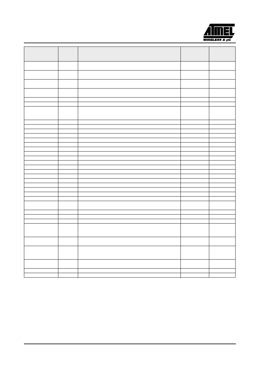
Signal Name
Type
Function
max. output
current [mA]
load [pF]
CMRD*
O/Z
Communication memory read strobe. This pin is asserted when the
TSS901E reads data from memory.
825
CMWR*
O/Z
Communication memory write strobe. This pin is asserted when
the TSS901E writes to data memory.
825
CMADR(15:0)
O/Z
Communication memory address. The TSS901E outputs an address
on these pins.
825
CMDATA(31:0)
IOZ
Communication memory data. The TSS901E inputs and outputs
data from and to com. memory on these pins.
350
COCI
I
Communication interface 'occupied' input signal
3
50
COCO
O/Z
Communication interface 'occupied' output signal
CAM
I
Communication interface arbitration master input signal
1: master
0: slave
CPUR*
O/Z
CPU Reset Signal
3
50
SES(3:0)*
O/Z
Specific External Signals
3
50
LDI1
I
Link Data Input channel 1
LSI1
I
Link Strobe Input channel 1
LDO1
O/Z
Link Data Output channel 1
12
25
LSO1
O/Z
Link Strobe Output channel 1
12
25
LEN1
O/Z
Link Enable Out (for external drivers)
3
50
LDI2
I
Link Data Input channel 2
LSI2
I
Link Strobe Input channel 2
LDO2
O/Z
Link Data Output channel 2
12
25
LSO2
O/Z
Link Strobe Output channel 2
12
25
LEN2
O/Z
Link Enable Out (for external drivers)
3
50
LDI3
I
Link Data Input channel 3
LSI3
I
Link Strobe Input channel 3
LDO3
O/Z
Link Data Output channel 3
12
25
LSO3
O/Z
Link Strobe Output channel 3
25
LEN3
O/Z
Link Enable Out (for external drivers)
3
50
TRST*
I
Test Reset. Resets the test state machine.
TCK
I
Test Clock. Provides an asynchronous clock for JTAG boundary
scan.
TMS
I
Test Mode Select. Used to control the test state machine.
TDI
I
Test Data Input. Provides serial data for the boundary scan logic.
TDO
O/Z
Test Data Output. Serial scan output of the boundary scan path.
3
50
RESET*
I
TSS901E Reset. Sets the TSS901E to a known state. This input
must be asserted (low) at power-up. The minimum width of RESET
low is 5 cycles of CLK10 in parallel with CLK running.
CLK
I
External clock input to TSS901E (max. 25 Mhz).
Must be derived from RAM access time.
CLK10
I
External clock input to TSS901E DS-links (application specific,
nominal 10 Mhz). Used to generate to transmission speed and link
disconnect timeout.
PLLOUT
O
Output of internal PLL. Used to connect a network of external RC
devices.
VCC
Power Supply
GND
Ground
相關(guān)PDF資料 |
PDF描述 |
|---|---|
| TSSH-106-01-L-D | 12 CONTACT(S), MALE, STRAIGHT TWO PART BOARD CONNECTOR, SOLDER |
| TSSH-108-01-T-DV | 16 CONTACT(S), MALE, STRAIGHT TWO PART BOARD CONNECTOR, SURFACE MOUNT |
| TSSH-112-01-S-D | 24 CONTACT(S), MALE, STRAIGHT TWO PART BOARD CONNECTOR, SOLDER |
| TSSH-113-01-L-DV-LC-M | 26 CONTACT(S), MALE, STRAIGHT TWO PART BOARD CONNECTOR, SURFACE MOUNT |
| TSSH-117-01-S-DV-LC | 34 CONTACT(S), MALE, STRAIGHT TWO PART BOARD CONNECTOR, SURFACE MOUNT |
相關(guān)代理商/技術(shù)參數(shù) |
參數(shù)描述 |
|---|---|
| TSS902EMA | 制造商:未知廠家 制造商全稱:未知廠家 功能描述:VITERBI DECODER|CMOS|QFL|132PIN|CERAMIC |
| TSS902EMA/883 | 制造商:未知廠家 制造商全稱:未知廠家 功能描述:VITERBI DECODER|CMOS|QFL|132PIN|CERAMIC |
| TSS902EMA-E | 制造商:未知廠家 制造商全稱:未知廠家 功能描述:VITERBI DECODER|CMOS|QFL|132PIN|CERAMIC |
| TSS902EMAP883 | 制造商:未知廠家 制造商全稱:未知廠家 功能描述:VITERBI DECODER|CMOS|QFL|132PIN|CERAMIC |
| TSS902EMAPIND | 制造商:未知廠家 制造商全稱:未知廠家 功能描述:VITERBI DECODER|CMOS|QFL|132PIN|CERAMIC |
發(fā)布緊急采購,3分鐘左右您將得到回復。