- 您現(xiàn)在的位置:買賣IC網(wǎng) > PDF目錄98307 > TZA1047HL/M3 (NXP SEMICONDUCTORS) SPECIALTY CONSUMER CIRCUIT, PQFP64 PDF資料下載
參數(shù)資料
| 型號(hào): | TZA1047HL/M3 |
| 廠商: | NXP SEMICONDUCTORS |
| 元件分類: | 消費(fèi)家電 |
| 英文描述: | SPECIALTY CONSUMER CIRCUIT, PQFP64 |
| 封裝: | 10 X 10 MM, 1.4 MM HEIGHT, PLASTIC, MS-026, SOT314-2, LQFP-64 |
| 文件頁(yè)數(shù): | 2/69頁(yè) |
| 文件大小: | 324K |
| 代理商: | TZA1047HL/M3 |
第1頁(yè)當(dāng)前第2頁(yè)第3頁(yè)第4頁(yè)第5頁(yè)第6頁(yè)第7頁(yè)第8頁(yè)第9頁(yè)第10頁(yè)第11頁(yè)第12頁(yè)第13頁(yè)第14頁(yè)第15頁(yè)第16頁(yè)第17頁(yè)第18頁(yè)第19頁(yè)第20頁(yè)第21頁(yè)第22頁(yè)第23頁(yè)第24頁(yè)第25頁(yè)第26頁(yè)第27頁(yè)第28頁(yè)第29頁(yè)第30頁(yè)第31頁(yè)第32頁(yè)第33頁(yè)第34頁(yè)第35頁(yè)第36頁(yè)第37頁(yè)第38頁(yè)第39頁(yè)第40頁(yè)第41頁(yè)第42頁(yè)第43頁(yè)第44頁(yè)第45頁(yè)第46頁(yè)第47頁(yè)第48頁(yè)第49頁(yè)第50頁(yè)第51頁(yè)第52頁(yè)第53頁(yè)第54頁(yè)第55頁(yè)第56頁(yè)第57頁(yè)第58頁(yè)第59頁(yè)第60頁(yè)第61頁(yè)第62頁(yè)第63頁(yè)第64頁(yè)第65頁(yè)第66頁(yè)第67頁(yè)第68頁(yè)第69頁(yè)

9397 750 14664
Koninklijke Philips Electronics N.V. 2005. All rights reserved.
Product data sheet
Rev. 02 — 1 June 2005
10 of 69
Philips Semiconductors
TZA1047
Preprocessor IC for CD and DVD rewritable
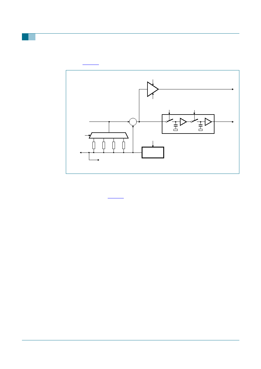
7.4 Input circuit
Refer to Figure 4.
The Input circuit comprises a voltage reference circuit, sample-and-hold circuit, and a
programmable gain amplier. The input signals to the Input circuit are VIA to VIH, and can
be either currents or voltages. The signal names correspond to the PDIC segments shown
termination resistor that is selectable by the control word LDSEG[1:0]. The currents of
input signals, for example from the TZA1045, are converted to voltages across the input
termination resistors.
The voltage reference circuit is a DAC which is programmable by control word VSEG[3:0]
to allow different PDICs to be supported. The voltage reference circuit has a sufciently
large sink capability for the 150
termination resistors, allowing the TZA1047 to work
with a characteristically terminated ex connection to the OPU.
Note that when the TZA1047 is in Standby mode (STBY = 1), VREF and the input resistors
remain active to allow the TZA1045 to deliver current to the TZA1047 without the risk of
‘latch-up’.
The reference voltage is subtracted from the input signals and the resulting signals VRA
to VRH are optionally sampled by a sample-and-hold circuit. The sampling signals TH1
and TH2 originate either directly from the codec IC or from the EFMTIM circuit. The
resultant signals VSA to VSH are sent to the Distributor for further processing. If sampling
is disabled (bit SMPLON = 0), both switches remain closed and the sample-and-hold
circuit is transparent.
The central signals VRA to VRD are amplied for DPD use at a gain programmable by
control word GSEG[1:0]. The resultant four signals VUA to VUD go to the DPD circuit. The
GSEG gain is enabled when bit DPD = 1 and is disabled, to save power, when bit
DPD=0.
The input signal range for VIA to VIH
V
ref is 1 V maximum.
Fig 4.
Input circuit.
001aab193
REFERENCE
CIRCUIT
TH1
DPD
GSEG
VSEG
TH2
SAMPLE-AND-HOLD (8
×)
+
VREF
VRA to VRH
VRA to VRD
VSA to VSH
VUA to VUD
LDSEG
VREF
VIA to VIH
R0
(8
×)
R1
(8
×)
R2
(8
×)
R3
(8
×)
相關(guān)PDF資料 |
PDF描述 |
|---|---|
| TZA1049TH | SPECIALTY CONSUMER CIRCUIT, PDSO28 |
| 1N5376ATR | TRANS PNP HV -300V -500MA TO-92 |
| 1N5376BTR | TRANS PNP HV -200V -1000MA TO-92 |
| 1N5376C | TRANS PNP HG -15V -3000MA TO-92 |
| 1N5376CTR | TRANS PNP HG -15V -2000MA TO-92 |
相關(guān)代理商/技術(shù)參數(shù) |
參數(shù)描述 |
|---|---|
| TZA1048 | 制造商:PHILIPS 制造商全稱:NXP Semiconductors 功能描述:4-channel BTL driver for CD/DVD drives |
| TZA1048TH | 制造商:PHILIPS 制造商全稱:NXP Semiconductors 功能描述:4-channel BTL driver for CD/DVD drives |
| TZA10-5 | 制造商:RHOMBUS-IND 制造商全稱:Rhombus Industries Inc. 功能描述:TZA / TYA Series 5-Tap High Performance Passive Delay Modules |
| TZA10-7 | 制造商:RHOMBUS-IND 制造商全稱:Rhombus Industries Inc. 功能描述:TZA / TYA Series 5-Tap High Performance Passive Delay Modules |
| TZA1-10 | 制造商:RHOMBUS-IND 制造商全稱:Rhombus Industries Inc. 功能描述:TZA / TYA Series 5-Tap High Performance Passive Delay Modules |
發(fā)布緊急采購(gòu),3分鐘左右您將得到回復(fù)。