- 您現(xiàn)在的位置:買賣IC網(wǎng) > PDF目錄225404 > UC3827Q-1 (TEXAS INSTRUMENTS INC) 1 A SWITCHING CONTROLLER, 500 kHz SWITCHING FREQ-MAX, PQCC28 PDF資料下載
參數(shù)資料
| 型號: | UC3827Q-1 |
| 廠商: | TEXAS INSTRUMENTS INC |
| 元件分類: | 穩(wěn)壓器 |
| 英文描述: | 1 A SWITCHING CONTROLLER, 500 kHz SWITCHING FREQ-MAX, PQCC28 |
| 封裝: | PLASIC, LCC-28 |
| 文件頁數(shù): | 12/16頁 |
| 文件大?。?/td> | 391K |
| 代理商: | UC3827Q-1 |

f
OSC +
0.77
R
RT
C
CT
(Hz)
t
DELAY +
R
DELAY
200W
10*9 (s)
1
2
3
4
5
6
7
8
9
10
11
12
24
23
22
21
20
19
18
17
16
15
14
13
V+
BUCK
SRC
SS
RAMP
CEAO
CSAO
CSA+
CSA
VEAO
GND
CEA+
PUSH
VCC
PULL
PGND
DELAY
SYNC
CT
RT
VEA
REF
VEA+
CEA
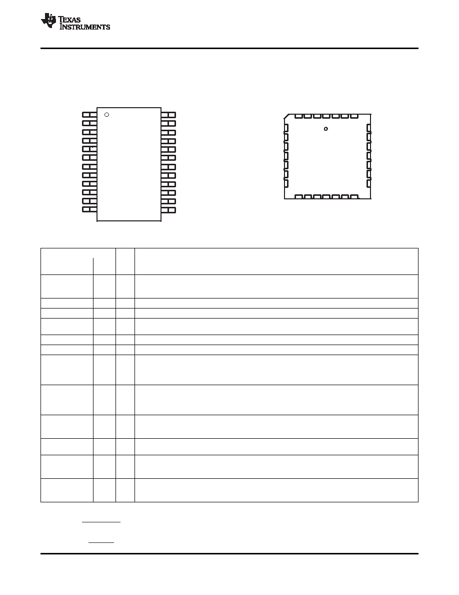
N, J OR DW PACKAGES
(TOP VIEW)
3 2 1
13 14
5
6
7
8
9
10
11
PGND
NC
DELAY
SYNC
CT
RT
SS
RAMP
CEAO
CSAO
CSA+
CSA
VEAO
4
15 16 17 18
CEA+
CEA
VEA+
REF
NC
VEA
SRC
BUCK
NC
V+
Q PACKAGE
(TOP VIEW)
28 27 26
25
24
23
22
21
20
19
12
GND
PUSH
VCC
PULL
NC No internal connection
(1)
(2)
SLUS365D
– APRIL 1999 – REVISED APRIL 2011
PLCC-28 (Q PACKAGE)
CONNECTION DIAGRAMS
(TOP VIEW)
DIL-24 (N or J, DW PACKAGES)
(TOP VIEW)
Terminal Functions
TERMINAL
I/O
DESCRIPTION
N or
NAME
Q
DW
Output of the buck PWM controller. The BUCK output is a floating driver, optimized for controlling the
BUCK
2
3
O
gate of an N-channel MOSFET. The peak sink and source currents are 1 A. VCC undervoltage faults
disables BUCK to an off condition (low).
CEA+
12
13
I
Non-inverting input of the current error amplifier.
CEA-
13
14
I
Inverting input of the current error amplifier
Output of the current error amplifier and the inverting input of the PWM comparator of the buck
CEAO
6
7
O
converter.
CSA+
8
9
I
Noninverting input of the current sense amplifier.
CSA
–
9
10
I
Inverting input of the current sense amplifier.
Output of the current sense amplifier and the noninverting input of the current limit comparator. When
the signal level on this pin exceeds the 3V threshold of the current limit comparator, the buck gate drive
CSAO
7
8
O
pulse is terminated. This feature is useful to implement cycle-by-cycle current limiting for the buck
converter.
Provides for the timing capacitor which is connected between CT and GND. The oscillator frequency is
set by CT and a resistor RT, connected between pin RT and GND. The CT discharge current is
CT
18
20
I
approximately 40 x the bias current through the resistor connected to RT. A practical maximum value for
the discharge current is 20 mA. The frequency of the oscillator is given by equation(1)
A resistor to GND programs the overlap time of the PUSH and PULL outputs of the UC3827-1 and the
DELAY
20
22
I
dead time of the PUSH and PULL outputs of the UC3827-2. The minimum value of the resistor, RDELAY,
is 18 k
. The delay or overlap time is given by equation(2)
Ground reference for all sensitive setup components not related to driving the outputs. They include all
GND
11
12
-
timing, voltage sense, current sense, and bypass components.
Ground connection for the PUSH and PULL outputs. PGND must be connected to GND at a single point
PGND
21
25
-
on the printed circuit board. This is imperative to prevent large, high frequency switching currents
flowing through the ground metalization inside the device.
Ground referenced output to drive an N-channel MOSFET. The PULL and the PUSH outputs are driving
PULL
22
26
O
the two switches of the push-pull converter with complementary signals at close to a 50% duty cycle.
Any undervoltage faults will disable PULL to an off condition (low).
Copyright
1999–2011, Texas Instruments Incorporated
5
相關(guān)PDF資料 |
PDF描述 |
|---|---|
| UC3842ADX | |
| UC3843ADX | |
| UC3843ADW | 1 A SWITCHING CONTROLLER, 500 kHz SWITCHING FREQ-MAX, PDSO16 |
| UC3843D1X | |
| UC3844D1X | |
相關(guān)代理商/技術(shù)參數(shù) |
參數(shù)描述 |
|---|---|
| UC3827Q-2 | 制造商:未知廠家 制造商全稱:未知廠家 功能描述:Current/Voltage-Mode SMPS Controller |
| UC3827QTR-1 | 制造商:TI 制造商全稱:Texas Instruments 功能描述:Buck Current/Voltage Fed Push-Pull PWM Controllers |
| UC3827QTR-2 | 制造商:未知廠家 制造商全稱:未知廠家 功能描述:Current/Voltage-Mode SMPS Controller |
| UC3828 | 制造商:未知廠家 制造商全稱:未知廠家 功能描述:新型電流型PWM芯片 |
| UC382-ADJ | 制造商:TI 制造商全稱:Texas Instruments 功能描述:FAST LDO LINEAR REGULATOR |
發(fā)布緊急采購,3分鐘左右您將得到回復(fù)。