- 您現(xiàn)在的位置:買賣IC網(wǎng) > PDF目錄225404 > UC3827Q-1 (TEXAS INSTRUMENTS INC) 1 A SWITCHING CONTROLLER, 500 kHz SWITCHING FREQ-MAX, PQCC28 PDF資料下載
參數(shù)資料
| 型號: | UC3827Q-1 |
| 廠商: | TEXAS INSTRUMENTS INC |
| 元件分類: | 穩(wěn)壓器 |
| 英文描述: | 1 A SWITCHING CONTROLLER, 500 kHz SWITCHING FREQ-MAX, PQCC28 |
| 封裝: | PLASIC, LCC-28 |
| 文件頁數(shù): | 14/16頁 |
| 文件大小: | 391K |
| 代理商: | UC3827Q-1 |

+
–
RT
CT
SYNC
S
R
VREF
2.5 V
OSCILLATOR
VREF
10 kW
1.4 V
2.5 V
2.9 V
0.5 V
RT
CT
VDG99086
I
RT +
2.5 V
R
RT
SLUS365D
– APRIL 1999 – REVISED APRIL 2011
APPLICATION INFORMATION
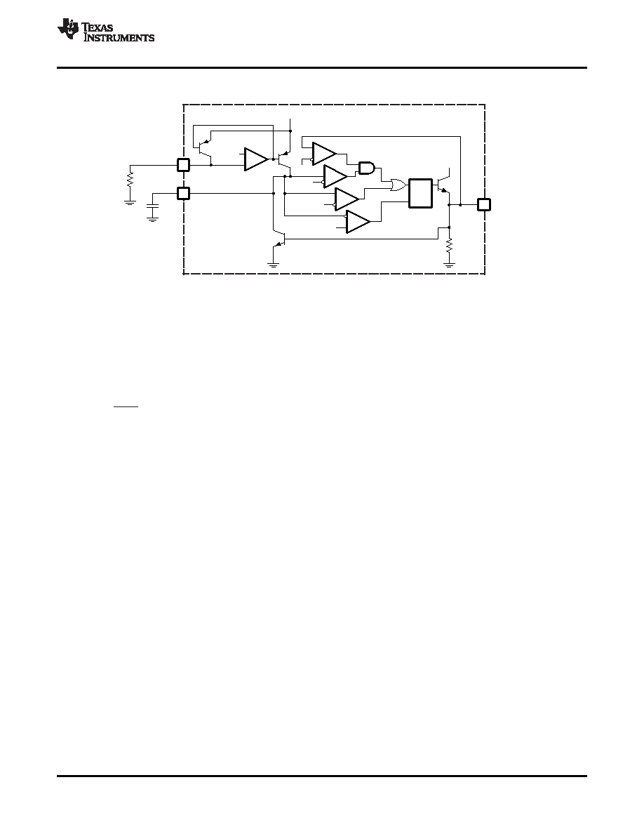
Figure 1. Oscillator Block With External Connections
CIRCUIT BLOCK DESCRIPTION
PWM Oscillator
The oscillator block diagram with external connections is shown in Equation 1. A resistor (RT) connected to pin
RT sets the linear charge current:
(1)
The timing capacitor (CCT) is linearly charged with the charge current forcing the OSC pin to charge to a 3.4 V
threshold. After exceeding this threshold, the RS flip-flop is set driving CLKSYN high and RDEAD low which
discharges CCT. CT continues to discharge until it reaches a 0.5 V threshold and resets the RS flip-flop which
repeats the charging sequence as shown in Figure 2
As shown in Figure 3, several oscillators are synchronized to the highest free running frequency by connecting
100 pF capacitors in series with each CLKSYN pin and connecting the other side of the capacitors together
forming the CLKSYN bus. The CLKSYN bus is then pulled down to ground with a resistance of approximately
10k. Referring to Figure 1, the synchronization threshold is 1.4 V. The oscillator blanks any synchronization pulse
that occurs when OSC is below 2.5 V. This allows units, once they discharge below 2.5 V, to continue through
the current discharge and subsequent charge cycles whether or not other units on the CLKSYN bus are still
synchronizing. This requires the frequency of all free running oscillators to be within 17% of each other to assure
synchronization.
Copyright
1999–2011, Texas Instruments Incorporated
7
相關PDF資料 |
PDF描述 |
|---|---|
| UC3842ADX | |
| UC3843ADX | |
| UC3843ADW | 1 A SWITCHING CONTROLLER, 500 kHz SWITCHING FREQ-MAX, PDSO16 |
| UC3843D1X | |
| UC3844D1X | |
相關代理商/技術參數(shù) |
參數(shù)描述 |
|---|---|
| UC3827Q-2 | 制造商:未知廠家 制造商全稱:未知廠家 功能描述:Current/Voltage-Mode SMPS Controller |
| UC3827QTR-1 | 制造商:TI 制造商全稱:Texas Instruments 功能描述:Buck Current/Voltage Fed Push-Pull PWM Controllers |
| UC3827QTR-2 | 制造商:未知廠家 制造商全稱:未知廠家 功能描述:Current/Voltage-Mode SMPS Controller |
| UC3828 | 制造商:未知廠家 制造商全稱:未知廠家 功能描述:新型電流型PWM芯片 |
| UC382-ADJ | 制造商:TI 制造商全稱:Texas Instruments 功能描述:FAST LDO LINEAR REGULATOR |
發(fā)布緊急采購,3分鐘左右您將得到回復。