- 您現(xiàn)在的位置:買賣IC網(wǎng) > PDF目錄379479 > UCC38517 (Texas Instruments, Inc.) ADVANCED PFC/PWM COMBINA CONTROLLERS PDF資料下載
參數(shù)資料
| 型號(hào): | UCC38517 |
| 廠商: | Texas Instruments, Inc. |
| 元件分類: | 基準(zhǔn)電壓源/電流源 |
| 英文描述: | ADVANCED PFC/PWM COMBINA CONTROLLERS |
| 中文描述: | 高級(jí)式PFC /脈寬調(diào)制COMBINA控制器 |
| 文件頁(yè)數(shù): | 7/39頁(yè) |
| 文件大小: | 725K |
| 代理商: | UCC38517 |
第1頁(yè)第2頁(yè)第3頁(yè)第4頁(yè)第5頁(yè)第6頁(yè)當(dāng)前第7頁(yè)第8頁(yè)第9頁(yè)第10頁(yè)第11頁(yè)第12頁(yè)第13頁(yè)第14頁(yè)第15頁(yè)第16頁(yè)第17頁(yè)第18頁(yè)第19頁(yè)第20頁(yè)第21頁(yè)第22頁(yè)第23頁(yè)第24頁(yè)第25頁(yè)第26頁(yè)第27頁(yè)第28頁(yè)第29頁(yè)第30頁(yè)第31頁(yè)第32頁(yè)第33頁(yè)第34頁(yè)第35頁(yè)第36頁(yè)第37頁(yè)第38頁(yè)第39頁(yè)
SLUS517B DECEMBER 2002 REVISED AUGUST 2004
7
www.ti.com
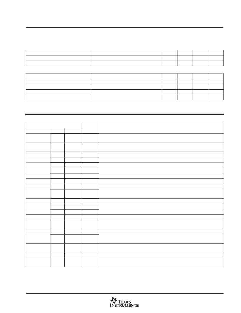
ELECTRICAL CHARACTERISTICS
T
A
= –40
°
C to 105
°
C for the UCC2851x, T
A
= T
J
, VCC = 12 V, R
T
= 156 k
,
R
CT_BUFF
= 10 k
(unless otherwise noted)
PWM stage overcurrent limit
PARAMETER
TEST CONDITIONS
MIN
TYP
MAX
UNITS
Peak current comparator threshold voltage
Input bias current(1)
1.15
1.30
1.45
V
50
nA
PWM stage gate driver
PARAMETER
TEST CONDITIONS
MIN
TYP
MAX
UNITS
ns
GT2 pull-up resistance
100 mA
≤
IOUT
≤
200 mA
IOUT = 100 mA
5
12
GT2 pull-down resistance
2
10
GT2 output rise time
CLOAD = 1 nF,
RLOAD = 10
16
25
GT2 output fall time
1. Ensured by design. Not 100% tested in production.
7
15
ns
TERMINAL FUNCTIONS
TERMINAL
I/O
DESCRIPTION
NAME
NO
.
Stage
CAOUT
15
PFC
O
Output of the current control amplifier of the PFC stage. CAOUT is internally connected
to the PWM comparator input in the PFC stage
CT_BUFF
5
PWM
O
Internally buffered PWM stage oscillator ramp output, typically used to program slope
compensation with a single resistor
D_MAX
4
PWM
I
Positive input to set the maximum duty cycle clamp level of the PWM stage
GND
6
Analog ground
GT1
12
PFC
O
PFC stage gate drive output
GT2
10
PWM
O
PWM stage gate drive output
IAC
18
PFC
I
Multiplier current input that is proportional to the instantaneous rectified line voltage
ISENSE1
16
PFC
I
Non-inverting input to the PFC stage current amplifier
ISENSE2
8
PWM
I
Input for PWM stage current sense and peak current limit
MOUT
17
PFC
I/O
PFC multiplier highimpedance current output, internally connected to the current am-
plifier inverting input
PKLMT
14
PFC
I
Voltage input to the PFC peak current limit comparator
PWRGND
11
Power ground for GT1, GT2 and high current return paths
RT
2
I
Oscillator programming pin that is set with a single resistor to GND
SS2
13
PWM
I
Soft start for the PWM stage
VAOUT
1
PFC
I/O
Output of the PFC transconductance voltage amplifier and it is internally connected to
the Zero Power Detect comparator input and the multiplier input
VCC
9
I
Positive supply voltage pin
VERR
7
PWM
I
Feedback error voltage input for the PWM stage, typically connected to an optocoupler
output
VFF
19
PFC
I
Voltage feedforward pin for the PFC stage, sources an IAC/2 current that should be
externally filtered
VREF
20
O
Precision 7.5-V reference output
VSENSE
3
PFC
I
Inverting input to the PFC transconductance voltage amplifier, and input to the OVP,
ENABLE and UVLO2 comparators
相關(guān)PDF資料 |
PDF描述 |
|---|---|
| UCC28517N | ADVANCED PFC/PWM COMBINATION CONTROLLERS |
| UCC2882-1 | Average Current Mode Synchronous Controller With 5-Bit DAC |
| UCC2882 | Average Current Mode Synchronous Controller With 5-Bit DAC |
| UCC2882- | Average Current Mode Synchronous Controller With 5-Bit DAC |
| UCC2975TRPW | Precision 500 mA regulators |
相關(guān)代理商/技術(shù)參數(shù) |
參數(shù)描述 |
|---|---|
| UCC38531 | 制造商:TI 制造商全稱:Texas Instruments 功能描述:Universal Serial Bus Power Controller |
| UCC3857 | 制造商:TI 制造商全稱:Texas Instruments 功能描述:Isolated Boost PFC Preregulator Controller |
| UCC3857N | 制造商:未知廠家 制造商全稱:未知廠家 功能描述:IC-PFC PRE-REGULATOR |
| UCC3858 | 制造商:TI 制造商全稱:Texas Instruments 功能描述:High Efficiency, High Power Factor Preregulator |
| UCC3858J | 制造商:未知廠家 制造商全稱:未知廠家 功能描述:Analog IC |
發(fā)布緊急采購(gòu),3分鐘左右您將得到回復(fù)。