- 您現(xiàn)在的位置:買賣IC網(wǎng) > PDF目錄378747 > UPD75312A (NEC Corp.) 4-BIT SINGLE-CHIP MICROCOMPUTER PDF資料下載
參數(shù)資料
| 型號(hào): | UPD75312A |
| 廠商: | NEC Corp. |
| 英文描述: | 4-BIT SINGLE-CHIP MICROCOMPUTER |
| 中文描述: | 4位單片機(jī) |
| 文件頁(yè)數(shù): | 16/62頁(yè) |
| 文件大小: | 577K |
| 代理商: | UPD75312A |
第1頁(yè)第2頁(yè)第3頁(yè)第4頁(yè)第5頁(yè)第6頁(yè)第7頁(yè)第8頁(yè)第9頁(yè)第10頁(yè)第11頁(yè)第12頁(yè)第13頁(yè)第14頁(yè)第15頁(yè)當(dāng)前第16頁(yè)第17頁(yè)第18頁(yè)第19頁(yè)第20頁(yè)第21頁(yè)第22頁(yè)第23頁(yè)第24頁(yè)第25頁(yè)第26頁(yè)第27頁(yè)第28頁(yè)第29頁(yè)第30頁(yè)第31頁(yè)第32頁(yè)第33頁(yè)第34頁(yè)第35頁(yè)第36頁(yè)第37頁(yè)第38頁(yè)第39頁(yè)第40頁(yè)第41頁(yè)第42頁(yè)第43頁(yè)第44頁(yè)第45頁(yè)第46頁(yè)第47頁(yè)第48頁(yè)第49頁(yè)第50頁(yè)第51頁(yè)第52頁(yè)第53頁(yè)第54頁(yè)第55頁(yè)第56頁(yè)第57頁(yè)第58頁(yè)第59頁(yè)第60頁(yè)第61頁(yè)第62頁(yè)
μ
PD75312(A), 75316(A)
16
3.5
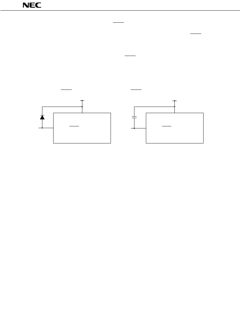
NOTES ON USING THE P00/INT4, AND RESET PINS
In addition to the functions described in Sections 3.1 and 3.2, an exclusive function for setting the test mode,
in which the internal fuctions of the
μ
PD75316(A) are tested, is provided to the P00/INT4 and RESET pins.
If a voltage exceeding V
DD
is applied to either of these pins, the
μ
PD75316(A) is put into test mode. Therefore,
even when the
μ
PD75316(A) is in normal operation, if noise exceeding the V
DD
is input into any of these pins,
the
μ
PD75316(A) will enter the test mode, and this will cause problems for normal operation.
As an example, if the wiring to the P00/INT4 pin or the RESET pin is long, stray noise may be picked up and
the above montioned problem may occur.
Therefore, all wiring to these pins must be made short enough to not pick up stray noise. If noise cannot
be avoided, suppress the noise using a capacitor or diode as shown in the figure below.
Connect a diode having a low V
F
across
P00/INT4 and RESET, and V
DD
.
Connect a capacitor across P00/INT4 and
RESET, and V
DD
.
4.
MEMORY CONFIGURATION
Program memory (ROM) ...16256
×
8 bits (0000H-3F7FH):
μ
PD75316(A)
...12160
×
8 bits (0000H-2F7FH):
μ
PD75312(A)
0000H, 0001H :
Vector table to which address from which program is started is written after
reset
0002H-000BH: Vector table to which address from which program is started is written after
interrupt
0020H-007FH: Table area referenced by GETI instruction
Data memory
Data area .... 512
×
4 bits (000H–1FFH)
Peripheral hardware area .... 128
×
4 bits (F80H–FFFH)
V
DD
V
DD
P00/INT4, RESET
V
DD
V
DD
P00/INT4, RESET
Low V
F
diode
相關(guān)PDF資料 |
PDF描述 |
|---|---|
| UPD75316 | 4-BIT SINGLE-CHIP MICROCOMPUTER |
| UPD75316A | 4-BIT SINGLE-CHIP MICROCOMPUTER |
| UPD75316GF | 4-BIT SINGLE-CHIP MICROCOMPUTER |
| UPD75336GC | DIODE ZENER SINGLE 500mW 51Vz 2.5mA-Izt 0.05 0.1uA-Ir 39Vr DO35-GLASS 5K/AMMO |
| UPD75336GK | 4-BIT SINGLE-CHIP MICROCOMPUTER |
相關(guān)代理商/技術(shù)參數(shù) |
參數(shù)描述 |
|---|---|
| UPD753204013 | 制造商:Panasonic Industrial Company 功能描述:IC |
| UPD7554AG-597-E2 | 制造商:Renesas Electronics Corporation 功能描述: |
| UPD7554AG-597-E2-A | 制造商:Renesas Electronics Corporation 功能描述: |
| UPD7554AG-603-E2 | 制造商:Renesas Electronics Corporation 功能描述: |
| UPD7554AG-603-E2-A | 制造商:Renesas Electronics Corporation 功能描述: |
發(fā)布緊急采購(gòu),3分鐘左右您將得到回復(fù)。