- 您現(xiàn)在的位置:買賣IC網(wǎng) > PDF目錄378748 > UPD780024A (NEC Corp.) 8-bit Microcontroller with 2/4/8K Bytes In-System Programmable Flash PDF資料下載
參數(shù)資料
| 型號: | UPD780024A |
| 廠商: | NEC Corp. |
| 元件分類: | 8位微控制器 |
| 英文描述: | 8-bit Microcontroller with 2/4/8K Bytes In-System Programmable Flash |
| 中文描述: | 8位微控制器與2/4/8K字節(jié)在系統(tǒng)可編程閃存 |
| 文件頁數(shù): | 7/90頁 |
| 文件大小: | 660K |
| 代理商: | UPD780024A |
第1頁第2頁第3頁第4頁第5頁第6頁當(dāng)前第7頁第8頁第9頁第10頁第11頁第12頁第13頁第14頁第15頁第16頁第17頁第18頁第19頁第20頁第21頁第22頁第23頁第24頁第25頁第26頁第27頁第28頁第29頁第30頁第31頁第32頁第33頁第34頁第35頁第36頁第37頁第38頁第39頁第40頁第41頁第42頁第43頁第44頁第45頁第46頁第47頁第48頁第49頁第50頁第51頁第52頁第53頁第54頁第55頁第56頁第57頁第58頁第59頁第60頁第61頁第62頁第63頁第64頁第65頁第66頁第67頁第68頁第69頁第70頁第71頁第72頁第73頁第74頁第75頁第76頁第77頁第78頁第79頁第80頁第81頁第82頁第83頁第84頁第85頁第86頁第87頁第88頁第89頁第90頁
μ
PD78F0034B, 78F0034BY, 78F0034B(A), 78F0034BY(A)
7
Data Sheet U16369EJ1V0DS
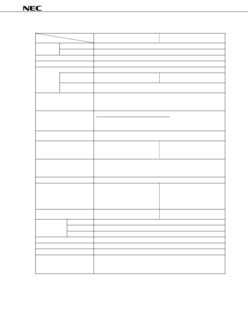
OVERVIEW OF FUNCTIONS
Part Number
μ
PD78F0034B
μ
PD78F0034B(A)
μ
PD78F0034BY
μ
PD78F0034BY(A)
Item
Internal
memory
Flash memory
32 KB
Note 1
High-speed RAM
1,024 bytes
Note 1
Memory space
64 KB
General-purpose registers
8 bits
×
32 registers (8 bits
×
8 registers
×
4 banks)
Minimum instruction execution time
On-chip minimum instruction execution time cycle variable function
When main system
0.166
μ
s/0.333
μ
s/0.666
μ
s/1.33
μ
s/2.66
μ
s
(@ 12 MHz operation, V
DD
= 4.5 to 5.5 V)
0.238
μ
s/0.48
μ
s/0.95
μ
s/1.91
μ
s/3.81
μ
s
(@ 8.38 MHz operation, V
DD
= 4.0 to 5.5 V)
When subsystem
clock selected
122
μ
s (@ 32.768 kHz operation)
Instruction set
16-bit operation
Multiply/divide (8 bits
×
8 bits, 16 bits
÷
8 bits)
Bit manipulation (set, reset, test, Boolean operation)
BCD adjust, etc.
I/O ports
Total:
51
CMOS input:
CMOS I/O:
N-ch open-drain I/O (5 V withstand voltage): 4
8
39
A/D converter
10-bit resolution
×
8 channels
Operable over a wide power supply voltage range: AV
DD
= 1.8 to 5.5 V
Serial interface
UART mode:
3-wire serial I/O mode: 2 channels
1 channel
UART mode:
3-wire serial I/O mode:
I
2
C bus mode
(multimaster supporting):1 channel
1 channel
1 channel
Timers
16-bit timer/event counter: 1 channel
8-bit timer/event counter:
Watch timer:
Watchdog timer:
2 channels
1 channel
1 channel
Timer outputs
3 (8-bit PWM output capable: 2)
Clock output
93.75 kHz, 187.5 kHz, 375 kHz, 750 kHz,
1.25 MHz, 3 MHz, 6 MHz, 12 MHz
(@ 12 MHz operation with main system
clock)
32.768 kHz (@ 32.768 kHz operation with
subsystem clock)
65.5 kHz, 131 kHz, 262 kHz, 524 kHz, 1.05
MHz, 2.10 MHz, 4.19 MHz, 8.38 MHz
(@ 8.38 MHz operation with main system
clock)
32.768 kHz (@ 32.768 kHz operation with
subsystem clock)
Buzzer output
1.46 kHz, 2.93 kHz, 5.86 kHz, 11.7 kHz
(@ 12 MHz operation with main system clock)
1.02 kHz, 2.05 kHz, 4.10 kHz, 8.19 kHz
(@ 8.38 MHz operation with main system clock)
Vectored interrupt
sources
Maskable
Internal: 13, external: 5
Non-maskable
Internal: 1
Software
1
Test inputs
Internal: 1, external: 1
Supply voltage
V
DD
= 1.8 to 5.5 V
Operating ambient temperature
T
A
=
–
40 to +85
°
C
Package
64-pin plastic LQFP (10 x 10)
64-pin plastic LQFP (14 x 14)
64-pin plastic TQFP (12 x 12)
73-pin plastic FBGA (9 x 9)
Note 2
Notes 1.
The capacities of the flash memory and the internal high-speed RAM can be changed with the memory
size switching register (IMS).
The special grade version of the 73-pin plastic FBGA (9 x 9) is not provided.
2.
相關(guān)PDF資料 |
PDF描述 |
|---|---|
| UPD780034A | 8-bit Microcontroller with 2/4/8K Bytes In-System Programmable Flash |
| UPD780021A | 8-BIT SINGLE-CHIP MICROCONTROLLERS |
| UPD780021AY | 8-BIT SINGLE-CHIP MICROCONTROLLERS |
| UPD780022A | 8-BIT SINGLE-CHIP MICROCONTROLLERS |
| UPD780022AY | 8-BIT SINGLE-CHIP MICROCONTROLLERS |
相關(guān)代理商/技術(shù)參數(shù) |
參數(shù)描述 |
|---|---|
| UPD780024AGK-C42-9ET | 制造商:Renesas Electronics Corporation 功能描述: |
| UPD780024AGK-C93-9ET | 制造商:Renesas Electronics Corporation 功能描述: |
| UPD780033AGK-B03-9ET | 制造商:Renesas Electronics Corporation 功能描述: |
| UPD780033AGK-B03-9ET-A | 制造商:Renesas Electronics Corporation 功能描述: |
| UPD780034AGC-119-8BS-A | 制造商:Renesas Electronics Corporation 功能描述:NECUPD780034AGC-119-8BS-A MCU |
發(fā)布緊急采購,3分鐘左右您將得到回復(fù)。