- 您現(xiàn)在的位置:買賣IC網(wǎng) > PDF目錄359411 > VP5311C (Zarlink Semiconductor Inc.) NTSC/PAL Digital Video Encoder PDF資料下載
參數(shù)資料
| 型號: | VP5311C |
| 廠商: | Zarlink Semiconductor Inc. |
| 英文描述: | NTSC/PAL Digital Video Encoder |
| 中文描述: | NTSC / PAL數(shù)字視頻編碼器 |
| 文件頁數(shù): | 9/19頁 |
| 文件大小: | 317K |
| 代理商: | VP5311C |

VP5311C/VP5511C
8
CCREG4
F2W2D6-0
Closed Caption register 4
Field two (line 284), second data byte
CC_CTL
F1ST
Closed Caption control register
Field one (line 21) status
High = data has been encoded
Low = new data has been loaded to
CCREG1-2
F2ST
Field two (line 284) status
High = data has been encoded
Low = new data has been loaded to
CCREG3-4
F1EN
Closed Caption field one (line 21)
High = enable
Low = disable (default)
F2EN
Closed Caption field two (line 284)
High = enable
Low = disable (default)
HSOFFM-L
HSOFF9-0
HS offset
This is a 10 bit number which allows the
user to offset the start of digital data input
with reference to the pulse HS.
SLAVE1
NCORSTD
H &V Slave mode control register
1 = NCO Line Reset Disable (NTSC only)
VBITDIS
0 = Video blanked when Rec656 V bit set
1 = V bit is ignored
0 = Standard Vsync I/P
1 = Even/Odd Field I/P
The odd and even fields are swapped
Selects pixel sample (0 to 3)
As HCNT7-0 but MSBs
H &V Slave position register
Adjusts for delay at which pixel data
occurs relative to HS
VSMODE
F_SWAP
SL_HS1-0
HCNT9-8
SLAVE2
HCNT7-0
GPSCTL
FSC4SEL
GPS Control
When high, REFSQ = 4xFSC and GPP
bit D6 is forced to become an input for a
SCSYNC signal (high = reset), which
provides a synchronous phase reset for
FSC divider. Low = normal operation with
REFSQ = 1xFSC. (default).
GENDITH
1 = Gen lock dither added.
GENLKEN
High = enable Genlock to REFSQ signal
input.
Low = internal subcarrier generation
(default).
NOLOCK
Genlock status bit (read only)
Low = Genlocked.
High = cannot lock to REFSQ. This bit is
cleared by reading and set again if lock
cannot be attained.
PALIDEN
High = enable external PAL ID phase
control and GPP bit D7 is forced to
become an input for PAL ID switch signal,
(GPP bit D7 - Low = +135
°
,High = -135
°
).
Low = normal operation, internal PAL ID
phase switch is used (default).
TSURST
High = chip soft reset. Registers are NOT
reset to default values.
Low = normal operation (default).
CHRMCLIP
High = enable clipping of chroma data
when luma goes below black level and is
clipped.
Low = no chroma clipping (default).
TRSEL
High = master mode, GPP bits D0 - 4 are
forced to become a video timing port with
VS, HS and FIELD outputs.
Low = slave mode, timing from REC656.
or H & V slave if SLH&V bit set
I
2
C BUS CONTROL INTERFACE
I
2
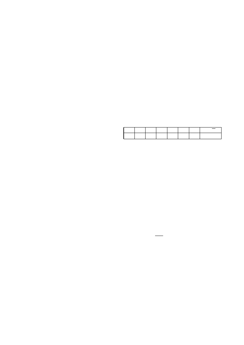
C bus address
A6
0
The serial microprocessor interface is via the bi-
directional port consisting of a data (SDA) and a clock (SCL)
line. It is compatible to the Philips I
2
C bus standard (Jan. 1992
publication number 9398 393 40011). The interface is a slave
transmitter - receiver with a sub-address capability. All
communication is controlled by the microprocessor. The SCL
line is input only. The most significant bit (MSB) is sent first.
Data must be stable during SCL high periods.
A bus free state is indicated by both SDA and SCL lines
being high. START of transmission is indicated by SDA being
pulled low while SCL is high. The end of transmission,
referred to as a STOP, is indicated by SDA going from low to
high while SCL is high. The STOP state can be omitted if a
repeated START is sent after the acknowledge bit. The
reading device acknowledges each byte by pulling the SDA
line low on the ninth clock pulse, after which the SDA line is
released to allow the transmitting device access to the bus.
The device address can be partially programmed by the
setting of the pins SA1 and SA2. This allows the device to
respond to one of four addresses, providing for system
flexibility. The I
2
C bus address is seven bits long with the last
bit indicating read / write for subsequent bytes.
The first data byte sent after the device address, is the
sub-address - BAR (base address register). The next byte will
be written to the register addressed by BAR and subsequent
bytes to the succeeding registers. The BAR maintains its data
after a STOP signal.
NTSC/PAL Video Standards
Both NTSC (4-field, 525 lines) and PAL (8-field, 625 lines)
video standards are supported by the VP5311C/VP5511C.
All raster synchronisation, colour sub-carrier and burst
characteristics are adapted to the standard selected. The
VP5311C/VP5511C generates outputs which follow the
requirements of SMPTE 170M and CCIR 624 for PAL signals.
The device supports the following:
NTSC,
PAL B, D, G, H, I, N (Argentina) and M.
A5
0
A4
0
A3
1
A2
1
A0
SA1
A1
SA2
R/
W
X
相關(guān)PDF資料 |
PDF描述 |
|---|---|
| VP531 | NTSC/PAL Digital Video Encoder |
| VP5513CG1N | NTSC/PAL Digital Video Encoder |
| VP5513GP1N | NTSC/PAL Digital Video Encoder |
| VP5513 | NTSC/PAL Digital Video Encoder |
| VP5513A1N | NTSC/PAL Digital Video Encoder |
相關(guān)代理商/技術(shù)參數(shù) |
參數(shù)描述 |
|---|---|
| VP5311C/CG/GP1N | 制造商:ZARLINK 制造商全稱:Zarlink Semiconductor Inc 功能描述:NTSC/PAL Digital Video Encoder |
| VP5311CCGGP1N | 制造商:未知廠家 制造商全稱:未知廠家 功能描述:Color Encoder Circuit |
| VP5311CG | 制造商:MITEL 制造商全稱:Mitel Networks Corporation 功能描述:NTSC/PAL Digital Video Encoder |
| VP5311D/CG/GP1N | 制造商:未知廠家 制造商全稱:未知廠家 功能描述:Color Encoder Circuit |
| VP5313 | 制造商:ZARLINK 制造商全稱:Zarlink Semiconductor Inc 功能描述:NTSC/PAL Digital Video Encoder |
發(fā)布緊急采購,3分鐘左右您將得到回復(fù)。