- 您現(xiàn)在的位置:買賣IC網(wǎng) > PDF目錄361773 > W238 Clocks and Buffers PDF資料下載
參數(shù)資料
| 型號: | W238 |
| 英文描述: | Clocks and Buffers |
| 中文描述: | 時(shí)鐘和緩沖器 |
| 文件頁數(shù): | 2/17頁 |
| 文件大?。?/td> | 175K |
| 代理商: | W238 |
W238
Document #: 38-07219 Rev. *A*
Page 2 of 17
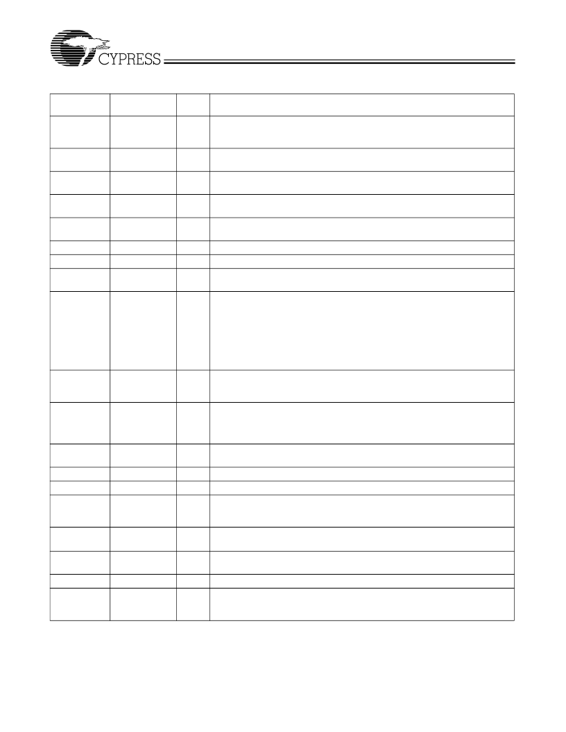
Pin Definitions
Pin Name
REF/FSEL1
Pin No.
4
Pin
Type
I/O
Pin Description
Reference Clock/Function Select:
3.3V 14.318-MHz clock output. This pin also
serves as a strap option for CPU frequency selection. See
Table 1
for detailed
descriptions.
Crystal Input:
This pin has dual functions. It can be used as an external
14.318-MHz crystal connection or as an external reference frequency input.
Crystal Output:
An input connection for an external 14.318-MHz crystal. If using
an external reference, this pin must be left unconnected.
PCI Clock 0 through 4:
3.3V 33-MHz PCI clock outputs. PCI1:4 can be individually
turned off via SMBus interface.
66-MHz Clock Output:
3.3V fixed 66-MHz clock.
X1
6
I
X2
7
I
PCI0_ICH,
PCI1:4
3V66_0:1
3V66_AGP
USB
DOT
FSEL0
14, 15, 16, 19,
20
10, 11, 12
O
O
28
29
21
O
O
I
USB Clock Output:
3.3V fixed 48-MHz, non-spread spectrum USB clock outputs.
Dot Clock Output:
3.3V 48-MHz, non-spread spectrum signal.
Clock Function Selection Pins:
LVTTL-compatible input to select device func-
tions. See
Table 1
for detailed descriptions.
TRISTATE#/PWRDWN#:
During power-up, this pin defaults to the TRISTATE# in-
put function to enable the TRISTATE# and test modes listed in Table 1. Approxi-
mately 1 ms to 2 ms after power on and the TRISTATE#/PWRDWN# input is HIGH,
this pin will change to the PWRDWN# input function and TRISTATE# functionality
is disabled. On the other hand, if the status of the TRISTATE#/PWRDWN# input
pin is LOW during power-on, this pin will be functioned as the TRISTATE# input
function until the input becomes HIGH and the function of this input pin will become
PWRDWN#.
CPU Clock Outputs:
Clock outputs for the host bus interface and integrated test
port. Output frequencies run at 66 MHz, 100 MHz, or 133 MHz, depending on the
configuration of FSEL0:1 and TRISTATE#. Voltage swing set by V
DDQ2
.
SDRAM Clock Outputs:
3.3V outputs running to 133 MHz. SDRAM0:7 can be
individually turned off via SMBus interface.
PWRDWN#/
TRISTATE#
30
I
CPU0:1
54, 53
O
SDRAM0:12
51, 50, 47, 46,
45, 44, 41, 40,
39, 38, 35, 34,
31
1
O
APIC
O
Synchronous APIC Clock Outputs:
Clock outputs running synchronous with the
PCI clock outputs (33 MHz). Voltage swing set by V
DDQ2
.
Data pin for SMBus circuitry.
Clock pin for SMBus circuitry.
3.3V Power Connection:
Power supply for SDRAM output buffers, PCI output
buffers, 3V66 output buffers, reference output buffers, and 48-MHz output buffers.
Connect to 3.3V.
3.3V Power Connection:
Power supply for core logic, PLL circuitry. Connect to
3.3V
.
2.5V Power Connection:
Power supply for IOAPIC and CPU output buffers. Con-
nect to 2.5V or 3.3V.
Ground Connections:
Ground for core logic, PLL circuitry
.
Ground Connections:
Connect all ground pins to the common system ground
plane.
SDATA
SCLK
VDDQ3
25
24
I/O
I
P
5, 9, 17, 27, 33,
37, 43, 49
VDDA
23
O
VDDQ2
2, 55
P
GNDA
GND
22
G
G
3, 8, 13, 18, 26,
32, 36, 42, 48,
52, 56
相關(guān)PDF資料 |
PDF描述 |
|---|---|
| W23C4096-12 | x8 ROM (Mask Programmable) |
| W23C4096-15 | x8 ROM (Mask Programmable) |
| W23C4096-20 | x8 ROM (Mask Programmable) |
| W23C8192-12 | x8 ROM (Mask Programmable) |
| W23C8192-15 | x8 ROM (Mask Programmable) |
相關(guān)代理商/技術(shù)參數(shù) |
參數(shù)描述 |
|---|---|
| W238-02 | 制造商:未知廠家 制造商全稱:未知廠家 功能描述:Clocks and Buffers |
| W238E32A | 制造商:OMRON INDUSTRIAL AUTOMATION 功能描述:Replaced by W238-E1-7 |
| W23C4096-12 | 制造商:未知廠家 制造商全稱:未知廠家 功能描述:x8 ROM (Mask Programmable) |
| W23C4096-15 | 制造商:未知廠家 制造商全稱:未知廠家 功能描述:x8 ROM (Mask Programmable) |
| W23C4096-20 | 制造商:未知廠家 制造商全稱:未知廠家 功能描述:x8 ROM (Mask Programmable) |
發(fā)布緊急采購,3分鐘左右您將得到回復(fù)。