- 您現(xiàn)在的位置:買賣IC網(wǎng) > PDF目錄231492 > W25X32-VSSI-Z (WINBOND ELECTRONICS CORP) 32M X 1 FLASH 2.7V PROM, PDSO8 PDF資料下載
參數(shù)資料
| 型號: | W25X32-VSSI-Z |
| 廠商: | WINBOND ELECTRONICS CORP |
| 元件分類: | PROM |
| 英文描述: | 32M X 1 FLASH 2.7V PROM, PDSO8 |
| 封裝: | 0.208 INCH, ROHS COMPLIANT, SOIC-8 |
| 文件頁數(shù): | 17/47頁 |
| 文件大?。?/td> | 1317K |
| 代理商: | W25X32-VSSI-Z |
第1頁第2頁第3頁第4頁第5頁第6頁第7頁第8頁第9頁第10頁第11頁第12頁第13頁第14頁第15頁第16頁當(dāng)前第17頁第18頁第19頁第20頁第21頁第22頁第23頁第24頁第25頁第26頁第27頁第28頁第29頁第30頁第31頁第32頁第33頁第34頁第35頁第36頁第37頁第38頁第39頁第40頁第41頁第42頁第43頁第44頁第45頁第46頁第47頁
W25X16, W25X32, W25X64
- 24 -
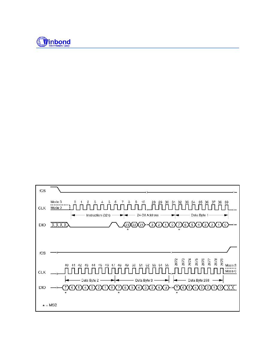
11.2.10 Page Program (02h)
The Page Program instruction allows up to 256 bytes of data to be programmed at previously erased
to all 1s (FFh) memory locations. A Write Enable instruction must be executed before the device will
accept the Page Program Instruction (Status Register bit WEL must equal 1). The instruction is
initiated by driving the /CS pin low then shifting the instruction code “02h” followed by a 24-bit address
(A23-A0) and at least one data byte, into the DIO pin. The /CS pin must be held low for the entire
length of the instruction while data is being sent to the device. The Page Program instruction
sequence is shown in figure 11.
If an entire 256 byte page is to be programmed, the last address byte (the 8 least significant address
bits) should be set to 0. If the last address byte is not zero, and the number of clocks exceed the
remaining page length, the addressing will wrap to the beginning of the page. In some cases, less
than 256 bytes (a partial page) can be programmed without having any effect on other bytes within the
same page. One condition to perform a partial page program is that the number of clocks can not
exceed the remaining page length. If more than 256 bytes are sent to the device the addressing will
wrap to the beginning of the page and overwrite previously sent data.
As with the write and erase instructions, the /CS pin must be driven high after the eighth bit of the last
byte has been latched. If this is not done the Page Program instruction will not be executed. After /CS
is driven high, the self-timed Page Program instruction will commence for a time duration of tpp (See
AC Characteristics). While the Page Program cycle is in progress, the Read Status Register
instruction may still be accessed for checking the status of the BUSY bit. The BUSY bit is a 1 during
the Page Program cycle and becomes a 0 when the cycle is finished and the device is ready to accept
other instructions again. After the Page Program cycle has finished the Write Enable Latch (WEL) bit
in the Status Register is cleared to 0. The Page Program instruction will not be executed if the
addressed page is protected by the Block Protect (BP2, BP1, and BP0) bits (see Status Register
Memory Protection table).
Figure 11. Page Program Instruction Sequence Diagram
相關(guān)PDF資料 |
PDF描述 |
|---|---|
| WF1024K32E-150H2M | 4M X 8 FLASH 12V PROM MODULE, 150 ns, CHIP66 |
| WS128K48-20G4WMA | 768K X 8 MULTI DEVICE SRAM MODULE, 20 ns, CQFP116 |
| WSF512K32-39G2TMA | SPECIALTY MEMORY CIRCUIT, CQFP68 |
| WS512K16-35DLIA | 512K X 16 MULTI DEVICE SRAM MODULE, 35 ns, CDMA44 |
| WS512K8-35CQ | 512K X 8 MULTI DEVICE SRAM MODULE, 35 ns, DMA32 |
相關(guān)代理商/技術(shù)參數(shù) |
參數(shù)描述 |
|---|---|
| W25X32VZEI | 制造商:WINBOND 制造商全稱:Winbond 功能描述:16M-BIT, 32M-BIT, AND 64M-BIT SERIAL FLASH MEMORY WITH 4KB SECTORS AND DUAL OUTPUT SPI |
| W25X32VZEIG | 功能描述:IC FLASH 32MBIT 75MHZ 8WSON RoHS:是 類別:集成電路 (IC) >> 存儲(chǔ)器 系列:SpiFlash® 標(biāo)準(zhǔn)包裝:1,000 系列:- 格式 - 存儲(chǔ)器:RAM 存儲(chǔ)器類型:移動(dòng) SDRAM 存儲(chǔ)容量:256M(8Mx32) 速度:133MHz 接口:并聯(lián) 電源電壓:1.7 V ~ 1.95 V 工作溫度:-40°C ~ 85°C 封裝/外殼:90-VFBGA 供應(yīng)商設(shè)備封裝:90-VFBGA(8x13) 包裝:帶卷 (TR) 其它名稱:557-1327-2 |
| W25X32VZEIG T&R | 功能描述:IC FLASH 32MBIT 75MHZ 8WSON RoHS:是 類別:集成電路 (IC) >> 存儲(chǔ)器 系列:SpiFlash® 標(biāo)準(zhǔn)包裝:1,000 系列:- 格式 - 存儲(chǔ)器:RAM 存儲(chǔ)器類型:移動(dòng) SDRAM 存儲(chǔ)容量:256M(8Mx32) 速度:133MHz 接口:并聯(lián) 電源電壓:1.7 V ~ 1.95 V 工作溫度:-40°C ~ 85°C 封裝/外殼:90-VFBGA 供應(yīng)商設(shè)備封裝:90-VFBGA(8x13) 包裝:帶卷 (TR) 其它名稱:557-1327-2 |
| W25X32VZEIZ | 制造商:WINBOND 制造商全稱:Winbond 功能描述:16M-BIT, 32M-BIT, AND 64M-BIT SERIAL FLASH MEMORY WITH 4KB SECTORS AND DUAL OUTPUT SPI |
| W25X32VZPI | 制造商:WINBOND 制造商全稱:Winbond 功能描述:16M-BIT, 32M-BIT, AND 64M-BIT SERIAL FLASH MEMORY WITH 4KB SECTORS AND DUAL OUTPUT SPI |
發(fā)布緊急采購,3分鐘左右您將得到回復(fù)。