- 您現在的位置:買賣IC網 > PDF目錄361789 > W65C816S8Q-14 16-Bit Microprocessor PDF資料下載
參數資料
| 型號: | W65C816S8Q-14 |
| 元件分類: | 16位微控制器 |
| 英文描述: | 16-Bit Microprocessor |
| 中文描述: | 16位微處理器 |
| 文件頁數: | 15/62頁 |
| 文件大小: | 891K |
| 代理商: | W65C816S8Q-14 |
第1頁第2頁第3頁第4頁第5頁第6頁第7頁第8頁第9頁第10頁第11頁第12頁第13頁第14頁當前第15頁第16頁第17頁第18頁第19頁第20頁第21頁第22頁第23頁第24頁第25頁第26頁第27頁第28頁第29頁第30頁第31頁第32頁第33頁第34頁第35頁第36頁第37頁第38頁第39頁第40頁第41頁第42頁第43頁第44頁第45頁第46頁第47頁第48頁第49頁第50頁第51頁第52頁第53頁第54頁第55頁第56頁第57頁第58頁第59頁第60頁第61頁第62頁
WESTERN DESIGN CENTER
W65C816S
March 1, 2000
15
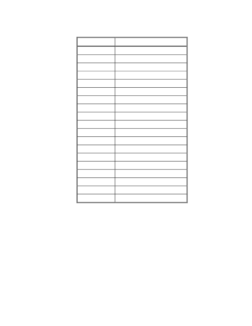
Table 2-1 Pin Function Table
Pin
Description
A0-A15
Address Bus
ABORTB
Abort Input
BE
Bus Enable
PHI2
Phase 2 In Clock
D0-D7/BA7
Data Bus/Bank Address Bus
E
Emulation Select
IRQB
Interrupt Request
MLB
Memory Lock
MX
Mode Select
NC
No Connect
NMIB
Non-Maskable Interrupt
RDY
Ready
RESB
Reset
RWB
Read/Write
VDA
Valid Data Address
VPB
Vector Pull
VPA
Valid Program Address
VDD
Positive Power Supply (+5 volts)
VSS
Internal Logic Ground
2.1
Abort (ABORTB)
The Abort input is used to abort instructions (usually due to an Address Bus condition). A negative transition
will inhibit modification of any internal register during the current instruction. Upon completion of this
instruction, an interrupt sequence is initiated. The location of the aborted OpCode is stored as the return address
in stack memory. The Abort vector address is 00FFF8,9 (Emulation mode) or 00FFE8,9 (Native mode). Note
that ABORTB is a pulse-sensitive signal; i.e., an abort will occur whenever there is a negative pulse (or level) on
the ABORTB pin during a PHI2 clock.
2.2
Address Bus (A0-A15)
These sixteen output lines form the Address Bus for memory and I/O exchange on the Data Bus. When using the
W65C816S, the address lines may be set to the high impedance state by the Bus Enable (BE) signal.
相關PDF資料 |
PDF描述 |
|---|---|
| W65C816SP10 | Microprocessor |
| W65C816SP-14 | 16-Bit Microprocessor |
| W65C816SPL10 | Microprocessor |
| W65C816SPL-14 | 16-Bit Microprocessor |
| W65C816SQ10 | Microprocessor |
相關代理商/技術參數 |
參數描述 |
|---|---|
| W65C816SP10 | 制造商:未知廠家 制造商全稱:未知廠家 功能描述:Microprocessor |
| W65C816SP-14 | 制造商:未知廠家 制造商全稱:未知廠家 功能描述:16-Bit Microprocessor |
| W65C816SPL10 | 制造商:未知廠家 制造商全稱:未知廠家 功能描述:Microprocessor |
| W65C816SPL-14 | 制造商:未知廠家 制造商全稱:未知廠家 功能描述:16-Bit Microprocessor |
| W65C816SQ10 | 制造商:未知廠家 制造商全稱:未知廠家 功能描述:Microprocessor |
發(fā)布緊急采購,3分鐘左右您將得到回復。