- 您現(xiàn)在的位置:買賣IC網(wǎng) > PDF目錄203637 > W946432AD-6 (WINBOND ELECTRONICS CORP) 2M X 32 DDR DRAM, 0.1 ns, PQFP100 PDF資料下載
參數(shù)資料
| 型號: | W946432AD-6 |
| 廠商: | WINBOND ELECTRONICS CORP |
| 元件分類: | DRAM |
| 英文描述: | 2M X 32 DDR DRAM, 0.1 ns, PQFP100 |
| 文件頁數(shù): | 23/39頁 |
| 文件大小: | 577K |
| 代理商: | W946432AD-6 |
第1頁第2頁第3頁第4頁第5頁第6頁第7頁第8頁第9頁第10頁第11頁第12頁第13頁第14頁第15頁第16頁第17頁第18頁第19頁第20頁第21頁第22頁當前第23頁第24頁第25頁第26頁第27頁第28頁第29頁第30頁第31頁第32頁第33頁第34頁第35頁第36頁第37頁第38頁第39頁
W946432AD
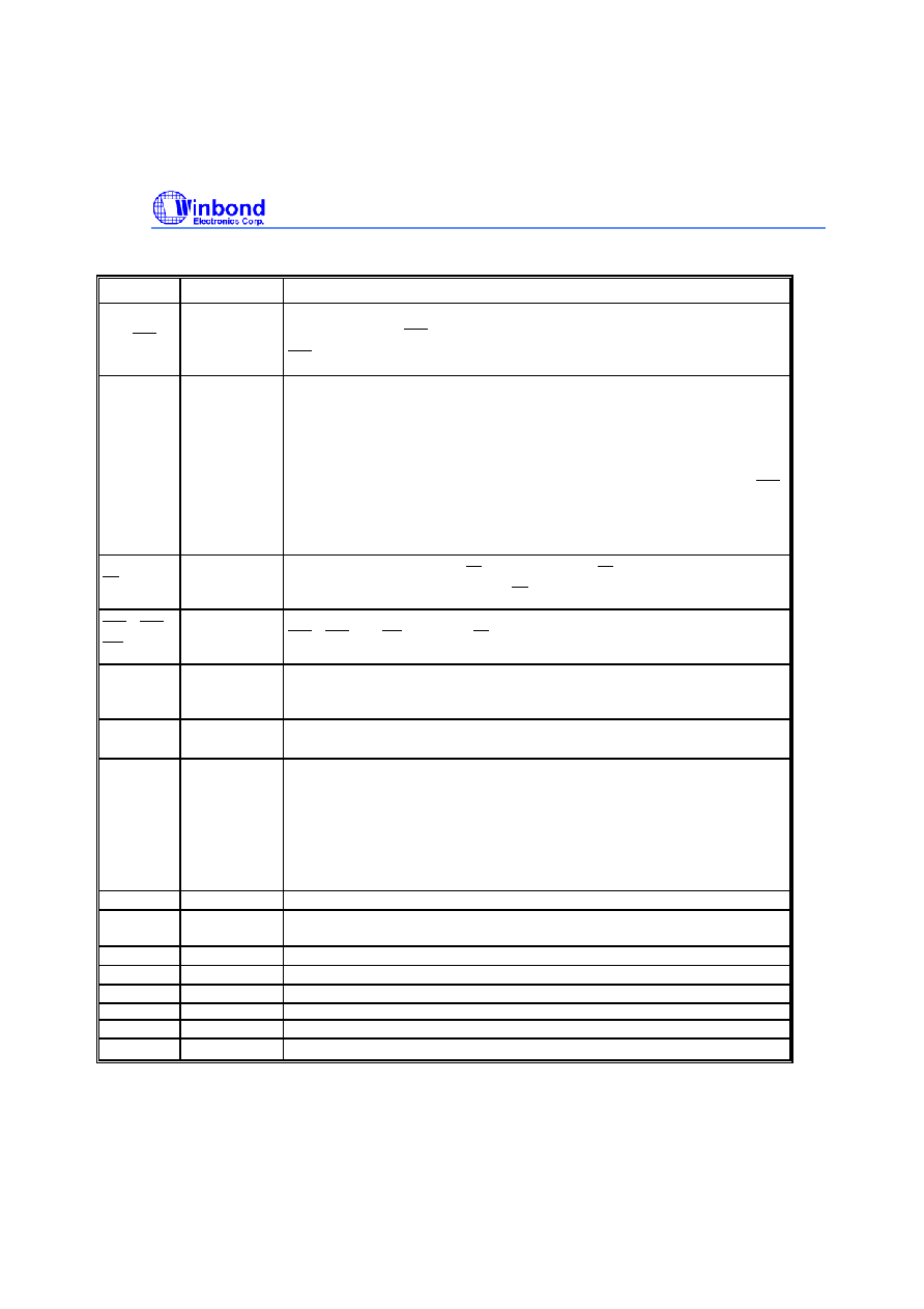
PIN DESCRIPTION
PIN NAME
FUNCTION
DESCRIPTION
CLK,
CLK
Differential clock
input
All address and control input signals are sampled on the crossing of the positive edge of CLK
and negative edge of CLK . Output (read) data is referenced to the crossings of CLK and
CLK (both directions of crossing).
CKE
Clock Enable
CKE HIGH activates, and CKE LOW deactivates internal clock signals, and device input
buffers and output drivers. Taking CKE LOW provides PRECHARGE POWER-DOWN and
SELF REFRESH operation (all banks idle), or ACTIVE POWER-DOWN (row ACTIVE in any
bank). CKE is synchronous for POWER-DOWN entry and exit, and for SELF REFRESH entry.
CKE is asynchronous for SELF REFRESH exit, and for output disable. CKE must be
maintained high throughout READ and WRITE accesses. Input buffers, excluding CLK, CLK
and CKE are disabled during POWER-DOWN. Input buffers, excluding CKE are disabled
during SELF REFRESH.
CS
Chip Select
All commands are masked when CS is registered HIGH. CS provides for external bank
selection on systems with multiple banks. CS is considered part of the command code.
RAS , CAS ,
WE
Command Inputs RAS , CAS and WE (along with CS ) define the command being entered.
DM
Input Data Mask
DM is an input mask signal for writes data. Input data is masked when DM is sampled HIGH
along with that input data during a WRITE access. DM is sampled on both edges of DQS.
Although DM pins are input only, the DM loading matches the DQ and DQS loading.
BA0, BA1
Bank Address
BA0 and BA1 define to which bank an ACTIVE, READ, WRITE or PRECHARGE command is
being applied.
A0-A10
Address Input
Provide the row address for ACTIVE commands, and the column address and AUTO
PRECHARGE bit for READ/WRITE commands, to select one location out of the memory array
in the respective bank. A8 is sampled during a PRECHARGE command to determine whether
the PRECHARGE applies to one bank (A8 LOW) or all banks (A8 HIGH). If only one bank is
to be precharged, the bank is selected by BA0, BA1. The address inputs also provide the op-
code during a MODE REGISTER SET command. BA0 and BA1 define which mode register is
loaded during the MODE REGISTER SET command (MRS or EMRS).
DQ
Data Input/Output Data bus
DQS
Data Strobe
Output with read data, input with write data. Edge-aligned with read data, centered in write
data. Used to capture write data.
VDDQ
DQ Power
For –5H VDDQ = 2.6V ± 0.1V, For –55/-6 VDDQ = 2.5V ± 0.6%
VSSQ
DQ Ground
Ground.
VDD
Supply Power
For –5H VDD = 2.6V ± 0.1V,For –55/-6 VDD = 2.5V ± 6%
VSS
Ground.
NC
No Connection
No connection
VREF
SSTL_2 reference voltage.
相關PDF資料 |
PDF描述 |
|---|---|
| W947D6HBHX6E | 8M X 16 DDR DRAM, 5 ns, PBGA60 |
| W9602BB | PUSHBUTTON SWITCH, SPST, MOMENTARY, 10A, 28VDC, PANEL MOUNT-THREADED |
| W9605BB | PUSHBUTTON SWITCH, SPST, MOMENTARY, 10A, 28VDC, PANEL MOUNT-THREADED |
| W9606BB | PUSHBUTTON SWITCH, SPDT, MOMENTARY, 10A, 28VDC, PANEL MOUNT-THREADED |
| W9712G8JB-3 | DDR DRAM, PBGA60 |
相關代理商/技術參數(shù) |
參數(shù)描述 |
|---|---|
| W9464G6IB | 制造商:WINBOND 制造商全稱:Winbond 功能描述:1M × 4 BANKS × 16 BITS DDR SDRAM |
| W9464G6IH | 制造商:WINBOND 制造商全稱:Winbond 功能描述:1M ?? 4 BANKS ?? 16 BITS DDR SDRAM |
| W9464G6JH | 制造商:WINBOND 制造商全稱:Winbond 功能描述:1M ? 4 BANKS ? 16 BITS DDR SDRAM |
| W9464G6JH-4 | 制造商:Winbond Electronics Corp 功能描述:IC DDR SDRAM 64M 200MHZ 66TSOP |
| W9464G6JH-5 | 制造商:Winbond Electronics Corp 功能描述:64MBIT DDRI 制造商:Winbond Electronics Corp 功能描述:IC DDR SDRAM 64M 200MHZ 66TSOP |
發(fā)布緊急采購,3分鐘左右您將得到回復。