- 您現(xiàn)在的位置:買賣IC網(wǎng) > PDF目錄371280 > X9241YVM Quad E2POT⑩ Nonvolatile Digital Potentiometer PDF資料下載
參數(shù)資料
| 型號: | X9241YVM |
| 元件分類: | 數(shù)字電位計 |
| 英文描述: | Quad E2POT⑩ Nonvolatile Digital Potentiometer |
| 中文描述: | 四E2POT⑩非易失數(shù)字電位器 |
| 文件頁數(shù): | 4/16頁 |
| 文件大?。?/td> | 76K |
| 代理商: | X9241YVM |

4
X9241
Instruction Structure
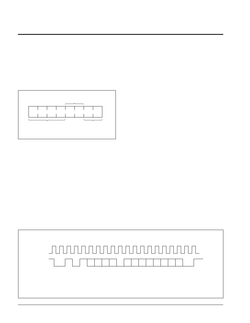
The next byte sent to the X9241 contains the instruction
and register pointer information. The four most signifi-
cant bits are the instruction. The next four bits point to
one of four pots and when applicable they point to one
of four associated registers. The format is shown below
in Figure 2.
action will be delayed t
STPWV
. A transfer from WCR
current wiper position, to a data register is a write to
nonvolatile memory and takes a minimum of t
WR
to
complete. The transfer can occur between one of the
four potentiometers and one of its associated registers;
or it may occur globally, wherein the transfer occurs
between all four of the potentiometers and one of their
associated registers.
Four instructions require a three-byte sequence to
complete. These instructions transfer data between the
host and the X9241; either between the host and one of
the data registers or directly between the host and the
WCR. These instructions are: Read WCR, read the
current wiper position of the selected pot; Write WCR,
change current wiper position of the selected pot; Read
Data Register, read the contents of the selected non-
volatile register; Write Data Register, write a new value
to the selected data register. The sequence of opera-
tions is shown in Figure 4.
The Increment/Decrement command is different from
the other commands. Once the command is issued and
the X9241 has responded with an acknowledge, the
master can clock the selected wiper up and/or down in
one segment steps; thereby, providing a fine tuning
capability to the host. For each SCL clock pulse (t
HIGH
)
while SDA is HIGH, the selected wiper will move one
resistor segment towards the V
H
terminal. Similarly, for
each SCL clock pulse while SDA is LOW, the selected
wiper will move one resistor segment towards the V
L
terminal. A detailed illustration of the sequence and
timing for this operation are shown in Figures 5 and 6
respectively.
Figure 3. Two-Byte Command Sequence
Figure 2. Instruction Byte Format
The four high order bits define the instruction. The next
two bits (P1 and P0) select which one of the four
potentiometers is to be affected by the instruction. The
last two bits (R1 and R0) select one of the four registers
that is to be acted upon when a register oriented instruc-
tion is issued.
Four of the nine instructions end with the transmission of
the instruction byte. The basic sequence is illustrated in
Figure 3. These two-byte instructions exchange data
between the WCR and one of the data registers. A
transfer from a data register to a WCR is essentially a
write to a static RAM. The response of the wiper to this
I1
3864 ILL F09.1
I2
I3
I0
P1
P0
R1
R0
POTENTIOMETER
SELECT
REGISTER
SELECT
INSTRUCTIONS
3864 ILL F10
S
T
A
R
T
0
1
0
1
A3
A2
A1
A0
A
C
K
I3
I2
I1
I0
P1
P0
R1 R0
A
C
K
SCL
SDA
S
T
O
P
相關PDF資料 |
PDF描述 |
|---|---|
| X9241UVM | Quad E2POT⑩ Nonvolatile Digital Potentiometer |
| X9251 | Quad Digitally-Controlled (XDCP) Potentiometer |
| X9251TB24 | Quad Digitally-Controlled (XDCP) Potentiometer |
| X9251TB24-2.7 | Quad Digitally-Controlled (XDCP) Potentiometer |
| X9251TB24I | Quad Digitally-Controlled (XDCP) Potentiometer |
相關代理商/技術參數(shù) |
參數(shù)描述 |
|---|---|
| X9250 | 制造商:INTERSIL 制造商全稱:Intersil Corporation 功能描述:Low Noise/Low Power/SPI Bus/256 Taps |
| X9250_06 | 制造商:INTERSIL 制造商全稱:Intersil Corporation 功能描述:Quad Digitally Controlled Potentiometers |
| X9250-2.7 | 制造商:INTERSIL 制造商全稱:Intersil Corporation 功能描述:Low Noise/Low Power/SPI Bus/256 Taps |
| X9250TB24 | 制造商:XICOR 制造商全稱:Xicor Inc. 功能描述:Quad Digitally Controlled Potentiometers (XDCP) |
| X9250TB24-2.7 | 制造商:XICOR 制造商全稱:Xicor Inc. 功能描述:Quad Digitally Controlled Potentiometers (XDCP) |
發(fā)布緊急采購,3分鐘左右您將得到回復。