- 您現(xiàn)在的位置:買賣IC網(wǎng) > PDF目錄371293 > X9400YZ24 Quad Digitally Controlled Potentiometers (XDCP) PDF資料下載
參數(shù)資料
| 型號: | X9400YZ24 |
| 元件分類: | 數(shù)字電位計(jì) |
| 英文描述: | Quad Digitally Controlled Potentiometers (XDCP) |
| 中文描述: | 四重?cái)?shù)控電位器(數(shù)字電位器) |
| 文件頁數(shù): | 2/22頁 |
| 文件大小: | 150K |
| 代理商: | X9400YZ24 |

X9400
Characteristics subject to change without notice.
2 of 22
REV 1.1.4 10/11/02
www.xicor.com
PIN DESCRIPTIONS
Host Interface Pins
Serial Output (SO)
SO is a push/pull serial data output pin. During a read
cycle, data is shifted out on this pin. Data is clocked
out by the falling edge of the serial clock.
Serial Input
SI is the serial data input pin. All opcodes, byte
addresses and data to be written to the pots and pot
registers are input on this pin. Data is latched by the
rising edge of the serial clock.
Serial Clock (SCK)
The SCK input is used to clock data into and out of the
X9400.
Chip Select (CS)
When CS is HIGH, the X9400 is deselected and the
SO pin is at high impedance, and (unless an internal
write cycle is underway) the device will be in the
standby state. CS LOW enables the X9400, placing it
in the active power mode. It should be noted that after
a power-up, a HIGH to LOW transition on CS is
required prior to the start of any operation.
Hold (HOLD)
HOLD is used in conjunction with the CS pin to select
the device. Once the part is selected and a serial
sequence is underway, HOLD may be used to pause
the serial communication with the controller without
resetting the serial sequence. To pause, HOLD must
be brought LOW while SCK is LOW. To resume
communication, HOLD is brought HIGH, again while
SCK is LOW. If the pause feature is not used, HOLD
should be held HIGH at all times.
Device Address (A
The address inputs are used to set the least significant
2 bits of the 8-bit slave address. A match in the slave
address serial data stream must be made with the
address input in order to initiate communication with
the X9400. A maximum of 4 devices may occupy the
SPI serial bus.
0
–
A
1
)
Potentiometer Pins
V
The V
terminal connections on either end of a mechanical
potentiometer.
H
/R
H
(V
/R
H0
/R
and V
H0
–V
H3
/R
/R
H3
inputs are equivalent to the
), V
L
/R
L
(V
L0
/R
L0
–V
L3
/R
L3
)
H
H
L
L
V
The wiper outputs are equivalent to the wiper output of
a mechanical potentiometer.
W
/R
W
(V
W0
/R
W0
–V
W3
/R
W3
)
Hardware Write Protect Input (WP)
The WP pin when LOW prevents nonvolatile writes to
the Data Registers.
Analog Supplies (V+, V-)
The analog Supplies V+, V- are the supply voltages for
the XDCP analog section.
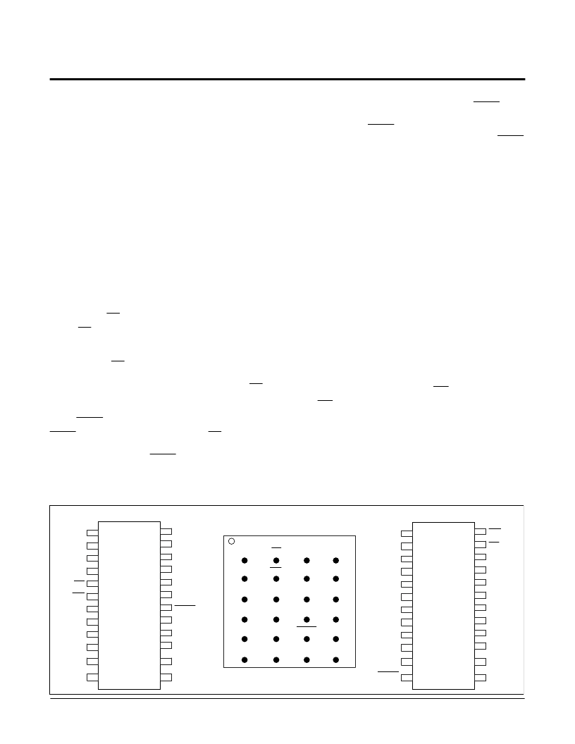
PIN CONFIGURATION
V
CC
V
L0
/R
L0
V
H0
/R
H0
V
W0
/R
W0
WP
SI
A
1
1
2
3
4
5
6
7
8
9
10
24
23
22
21
20
19
18
17
16
15
V+
V
L3
/R
L3
V
H3
/R
H3
V
W3
/R
W3
A
0
SO
HOLD
SCK
V
L2
/R
L2
V
H2
/R
H2
SOIC
X9408
V
SS
14
13
11
12
CS
V
L1
/R
L1
V
H1
/R
H1
V
W1
/R
W1
V
W2
/R
W2
V-
SI
A
1
V
H2
/R
H2
V
L2
/R
L2
1
2
3
4
5
6
7
8
9
10
24
23
22
21
20
19
18
17
16
15
WP
CS
V
W0
/R
W0
V
H0
/R
H0
V
L0
/R
L0
V
CC
V+
V
L3
/R
L3
V
H3
/R
H3
V
W3
/R
W3
TSSOP
X9408
V
W2
/R
W2
14
13
11
12
HOLD
V
L1
/R
L1
V
H1
/R
H1
V
W1
/R
W1
A
0
SO
V-
SCK
V
SS
2
3
4
A
B
C
D
E
F
Top View–Bumps Down
V
W0
/R
W0
V
L0
/R
L0
V+
A
0
HOLD
V
L1
/R
L1
V
CC
V
L3
/R
L3
V
W3
/R
W3
SO
SI
V
W1
/R
W1
SCK
V
L2
/R
L2
WP
V-
V
H0
/R
H0
V
H1
/R
H1
V
H3
/R
H3
V
H2
/R
H2
V
SS
V
W2
/R
W2
CS
A
1
1
XBGA
相關(guān)PDF資料 |
PDF描述 |
|---|---|
| X9400YZ24I-2.7 | Quad Digitally Controlled Potentiometers (XDCP) |
| X9400 | RF/Microwave Capacitor; Capacitance:20pF; Capacitance Tolerance:+/- 5%; Series:MC; Capacitor Dielectric Material:Mica; Termination:SMD; Leaded Process Compatible:No; Peak Reflow Compatible (260 C):No RoHS Compliant: No |
| X9400WP24 | Digital Potentiometer |
| X9400WP24-2.7 | Digital Potentiometer |
| X9400WP24I | Digital Potentiometer |
相關(guān)代理商/技術(shù)參數(shù) |
參數(shù)描述 |
|---|---|
| X9400YZ24I-2.7 | 制造商:XICOR 制造商全稱:Xicor Inc. 功能描述:Quad Digitally Controlled Potentiometers (XDCP) |
| X9401 | 制造商:INTERSIL 制造商全稱:Intersil Corporation 功能描述:Low Noise/Low Power/SPI Bus |
| X9401_06 | 制造商:INTERSIL 制造商全稱:Intersil Corporation 功能描述:Quad, 64 Tap, Digitally Controlled Potentiometer |
| X9401_09 | 制造商:INTERSIL 制造商全稱:Intersil Corporation 功能描述:Quad, 64 Tap, Digitally Controlled Potentiometer (XDCP?) |
| X94012011-01 | 功能描述:以太網(wǎng)模塊 XPress-Pro SW 94012F 8-Port 10/100TX RoHS:否 制造商:Lantronix 產(chǎn)品:Device Servers 數(shù)據(jù)速率:300 bps to 921.6 kbps, 10 Mbps, 100 Mbps 接口類型:Ethernet, Serial 工作電源電壓:5 V to 15 V 工作電源電流:133 mA to 400 mA 最大工作溫度:+ 70 C |
發(fā)布緊急采購,3分鐘左右您將得到回復(fù)。