- 您現(xiàn)在的位置:買賣IC網(wǎng) > PDF目錄4275 > XC2S200-6FG456C (Xilinx Inc)IC FPGA 2.5V C-TEMP 456-FBGA PDF資料下載
參數(shù)資料
| 型號(hào): | XC2S200-6FG456C |
| 廠商: | Xilinx Inc |
| 文件頁(yè)數(shù): | 26/99頁(yè) |
| 文件大?。?/td> | 0K |
| 描述: | IC FPGA 2.5V C-TEMP 456-FBGA |
| 標(biāo)準(zhǔn)包裝: | 60 |
| 系列: | Spartan®-II |
| LAB/CLB數(shù): | 1176 |
| 邏輯元件/單元數(shù): | 5292 |
| RAM 位總計(jì): | 57344 |
| 輸入/輸出數(shù): | 284 |
| 門數(shù): | 200000 |
| 電源電壓: | 2.375 V ~ 2.625 V |
| 安裝類型: | 表面貼裝 |
| 工作溫度: | 0°C ~ 85°C |
| 封裝/外殼: | 456-BBGA |
| 供應(yīng)商設(shè)備封裝: | 456-FBGA |
第1頁(yè)第2頁(yè)第3頁(yè)第4頁(yè)第5頁(yè)第6頁(yè)第7頁(yè)第8頁(yè)第9頁(yè)第10頁(yè)第11頁(yè)第12頁(yè)第13頁(yè)第14頁(yè)第15頁(yè)第16頁(yè)第17頁(yè)第18頁(yè)第19頁(yè)第20頁(yè)第21頁(yè)第22頁(yè)第23頁(yè)第24頁(yè)第25頁(yè)當(dāng)前第26頁(yè)第27頁(yè)第28頁(yè)第29頁(yè)第30頁(yè)第31頁(yè)第32頁(yè)第33頁(yè)第34頁(yè)第35頁(yè)第36頁(yè)第37頁(yè)第38頁(yè)第39頁(yè)第40頁(yè)第41頁(yè)第42頁(yè)第43頁(yè)第44頁(yè)第45頁(yè)第46頁(yè)第47頁(yè)第48頁(yè)第49頁(yè)第50頁(yè)第51頁(yè)第52頁(yè)第53頁(yè)第54頁(yè)第55頁(yè)第56頁(yè)第57頁(yè)第58頁(yè)第59頁(yè)第60頁(yè)第61頁(yè)第62頁(yè)第63頁(yè)第64頁(yè)第65頁(yè)第66頁(yè)第67頁(yè)第68頁(yè)第69頁(yè)第70頁(yè)第71頁(yè)第72頁(yè)第73頁(yè)第74頁(yè)第75頁(yè)第76頁(yè)第77頁(yè)第78頁(yè)第79頁(yè)第80頁(yè)第81頁(yè)第82頁(yè)第83頁(yè)第84頁(yè)第85頁(yè)第86頁(yè)第87頁(yè)第88頁(yè)第89頁(yè)第90頁(yè)第91頁(yè)第92頁(yè)第93頁(yè)第94頁(yè)第95頁(yè)第96頁(yè)第97頁(yè)第98頁(yè)第99頁(yè)

Spartan-II FPGA Family: Functional Description
DS001-2 (v2.8) June 13, 2008
Module 2 of 4
Product Specification
32
R
Using Block RAM Features
The Spartan-II FPGA family provides dedicated blocks of
on-chip, true dual-read/write port synchronous RAM, with
4096 memory cells. Each port of the block RAM memory
can be independently configured as a read/write port, a
read port, a write port, and can be configured to a specific
data width. The block RAM memory offers new capabilities
allowing the FPGA designer to simplify designs.
Operating Modes
Block RAM memory supports two operating modes.
Read Through
Write Back
Read Through (One Clock Edge)
The read address is registered on the read port clock edge
and data appears on the output after the RAM access time.
Some memories may place the latch/register at the outputs
depending on the desire to have a faster clock-to-out versus
setup time. This is generally considered to be an inferior
solution since it changes the read operation to an
asynchronous function with the possibility of missing an
address/control line transition during the generation of the
read pulse clock.
Write Back (One Clock Edge)
The write address is registered on the write port clock edge
and the data input is written to the memory and mirrored on
the write port input.
Block RAM Characteristics
1.
All inputs are registered with the port clock and have a
setup to clock timing specification.
2.
All outputs have a read through or write back function
depending on the state of the port WE pin. The outputs
relative to the port clock are available after the
clock-to-out timing specification.
3.
The block RAM are true SRAM memories and do not
have a combinatorial path from the address to the
output. The LUT cells in the CLBs are still available with
this function.
4.
The ports are completely independent from each other
(i.e., clocking, control, address, read/write function, and
data width) without arbitration.
5.
A write operation requires only one clock edge.
6.
A read operation requires only one clock edge.
The output ports are latched with a self timed circuit to
guarantee a glitch free read. The state of the output port will
not change until the port executes another read or write
operation.
Library Primitives
RAM primitives. Table 11 describes all of the available
primitives for synthesis and simulation.
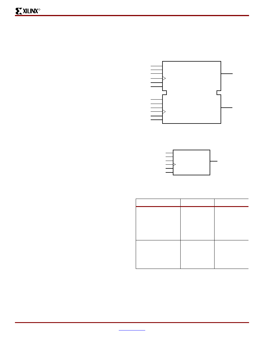
Figure 31: Dual-Port Block RAM Memory
Figure 32: Single-Port Block RAM Memory
Table 11: Available Library Primitives
Primitive
Port A Width
Port B Width
RAMB4_S1
RAMB4_S1_S1
RAMB4_S1_S2
RAMB4_S1_S4
RAMB4_S1_S8
RAMB4_S1_S16
1N/A
1
2
4
8
16
RAMB4_S2
RAMB4_S2_S2
RAMB4_S2_S4
RAMB4_S2_S8
RAMB4_S2_S16
2N/A
2
4
8
16
WEB
ENB
RSTB
CLKB
ADDRB[#:0]
DIB[#:0]
WEA
ENA
RSTA
CLKA
ADDRA[#:0]
DIA[#:0]
DOA[#:0]
DOB[#:0]
RAMB4_S#_S#
DS001_31_061200
DS001_32_061200
DO[#:0]
WE
EN
RST
CLK
ADDR[#:0]
DI[#:0]
RAMB4_S#
相關(guān)PDF資料 |
PDF描述 |
|---|---|
| AMM25DTMI | CONN EDGECARD 50POS R/A .156 SLD |
| 3341-31BULK | CONN JACKSOCKET M2.5/4-40 0.40" |
| XC2S200-5FG456I | IC FPGA 2.5V I-TEMP 456-FBGA |
| AMM25DTAI | CONN EDGECARD 50POS R/A .156 SLD |
| XC3S700A-5FGG484C | IC SPARTAN-3A FPGA 700K 484FBGA |
相關(guān)代理商/技術(shù)參數(shù) |
參數(shù)描述 |
|---|---|
| XC2S200-6FG456I | 制造商:XILINX 制造商全稱:XILINX 功能描述:Spartan-II 2.5V FPGA Family:Introduction and Ordering Information |
| XC2S200-6FGG256C | 制造商:Xilinx 功能描述:FPGA SPARTAN-II 200K GATES 5292 CELLS 263MHZ 2.5V 256FBGA - Trays 制造商:Xilinx 功能描述:FPGA 256 BGA SPARTAN II 制造商:Xilinx 功能描述:IC FPGA 176 I/O 256FBGA |
| XC2S200-6FGG256C4124 | 制造商:Xilinx 功能描述: |
| XC2S200-6FGG256I | 制造商:XILINX 制造商全稱:XILINX 功能描述:Spartan-II FPGA Family |
| XC2S200-6FGG456C | 功能描述:IC SPARTAN-II FPGA 200K 456-FBGA RoHS:是 類別:集成電路 (IC) >> 嵌入式 - FPGA(現(xiàn)場(chǎng)可編程門陣列) 系列:Spartan®-II 標(biāo)準(zhǔn)包裝:40 系列:Spartan® 6 LX LAB/CLB數(shù):3411 邏輯元件/單元數(shù):43661 RAM 位總計(jì):2138112 輸入/輸出數(shù):358 門數(shù):- 電源電壓:1.14 V ~ 1.26 V 安裝類型:表面貼裝 工作溫度:-40°C ~ 100°C 封裝/外殼:676-BGA 供應(yīng)商設(shè)備封裝:676-FBGA(27x27) |
發(fā)布緊急采購(gòu),3分鐘左右您將得到回復(fù)。