- 您現(xiàn)在的位置:買賣IC網(wǎng) > PDF目錄16988 > XRD98L61ZEVAL (Exar Corporation)EVAL BOARD FOR XRD98L61AIV PDF資料下載
參數(shù)資料
| 型號(hào): | XRD98L61ZEVAL |
| 廠商: | Exar Corporation |
| 文件頁數(shù): | 24/38頁 |
| 文件大?。?/td> | 0K |
| 描述: | EVAL BOARD FOR XRD98L61AIV |
| 標(biāo)準(zhǔn)包裝: | 1 |
| 系列: | * |
第1頁第2頁第3頁第4頁第5頁第6頁第7頁第8頁第9頁第10頁第11頁第12頁第13頁第14頁第15頁第16頁第17頁第18頁第19頁第20頁第21頁第22頁第23頁當(dāng)前第24頁第25頁第26頁第27頁第28頁第29頁第30頁第31頁第32頁第33頁第34頁第35頁第36頁第37頁第38頁

XRD98L61
30
Rev. 2.00
LINE RATE CLOCKS
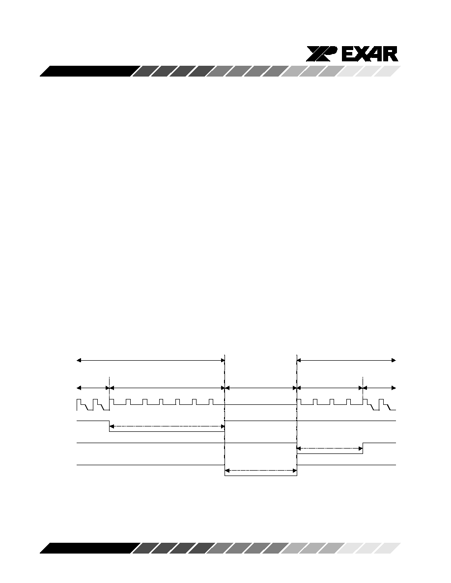
CLAMP & CAL are the two line rate clock signals.
There are two modes of operation for these clocks.
CAL & CLAMP Mode
In this mode, the CLAMP signal is used to activate the
DC restore Clamp at the CDS input, and the CAL signal
is used to define the Optical Black pixels to be used for
the Black Level calibration function. Typically the
CLAMP pulse comes during the dummy or optical
black pixels at the beginning of each scan line, and the
CAL pulse comes during the longer string of optical
black pixels at the end of each scan line. CLAMP &
CAL must not be active at the same time.
VS Reject Option (CAL & CLAMP Mode)
In the CAL and CLAMP mode, there is an option to
disconnect the CDS from the input pins during the
Vertical Shift time. To enable this option, write a “1” to
the VSreject bit in the Clock register. To properly define
the Vertical Shift time, you must set the ClampCal bit
properly.
In the typical case, the CCD has a few OB pixels at the
beginning of a line (CLAMP time) and a larger number
of OB pixels at the end of a scan line (CAL time). In this
case set the ClampCal bit = 0. This will define the
Vertical shift time as the time from the end of the CAL
pulse to the beginning of the CLAMP pulse.
If a CCD has more OB pixels at the beginning of a line,
then CAL should be active during these pixels and
CLAMP should be active at the end of the line. In this
case, set the ClampCal bit = 1. This will define the
Vertical shift time as the time from the end of the
CLAMP pulse to the beginning of the CAL pulse.
End of Line N
Start of Line N+1
Active Video
Pixels
OB pixels
Vertical Shift
Dummy &
OB pixels
CAL
(Black Level)
CLAMP
(DC restore)
CCD
Signal
Active Video pixels
t
CAL
t
CLAMP
Vert. Shift Reject
(internal)
Disconnect CDS from
input pins
Figure 20. Line Rate Timing with OneShot=0, VSreject=1 & ClampCal=0
相關(guān)PDF資料 |
PDF描述 |
|---|---|
| LGU2G391MELB | CAP ALUM 390UF 400V 20% SNAP |
| ECC31DCMT | CONN EDGECARD 62POS .100 WW |
| 1589448-3 | STRIP CON |
| AD8335-EVALZ | BOARD EVALUATION FOR AD8335 |
| RSM06DRSI-S288 | CONN EDGECARD 12POS DIP .156 SLD |
相關(guān)代理商/技術(shù)參數(shù) |
參數(shù)描述 |
|---|---|
| XRD98L62 | 制造商:EXAR 制造商全稱:EXAR 功能描述:CCD Image Digitizers with CDS, PGA and 12-Bit A/D |
| XRD98L62ACV | 制造商:EXAR 制造商全稱:EXAR 功能描述:CCD Image Digitizers with CDS, PGA and 12-Bit A/D |
| XRD98L62ACV-F | 功能描述:視頻 IC RoHS:否 制造商:Fairchild Semiconductor 工作電源電壓:5 V 電源電流:80 mA 最大工作溫度:+ 85 C 封裝 / 箱體:TSSOP-28 封裝:Reel |
| XRD98L62EVAL | 功能描述:數(shù)據(jù)轉(zhuǎn)換 IC 開發(fā)工具 XRD98L62 EVAL BOARD RoHS:否 制造商:Texas Instruments 產(chǎn)品:Demonstration Kits 類型:ADC 工具用于評(píng)估:ADS130E08 接口類型:SPI 工作電源電壓:- 6 V to + 6 V |
| XRD98L62ZEVAL | 功能描述:數(shù)據(jù)轉(zhuǎn)換 IC 開發(fā)工具 Eval Board (Solder) XRD98L62AIV RoHS:否 制造商:Texas Instruments 產(chǎn)品:Demonstration Kits 類型:ADC 工具用于評(píng)估:ADS130E08 接口類型:SPI 工作電源電壓:- 6 V to + 6 V |
發(fā)布緊急采購(gòu),3分鐘左右您將得到回復(fù)。