- 您現(xiàn)在的位置:買賣IC網(wǎng) > PDF目錄10001 > XRT7295AEIWTR (Exar Corporation)IC E3 LINE RECEIVER 20SOJ PDF資料下載
參數(shù)資料
| 型號: | XRT7295AEIWTR |
| 廠商: | Exar Corporation |
| 文件頁數(shù): | 2/15頁 |
| 文件大小: | 0K |
| 描述: | IC E3 LINE RECEIVER 20SOJ |
| 標(biāo)準(zhǔn)包裝: | 1,000 |
| 類型: | 接收器 |
| 驅(qū)動器/接收器數(shù): | 0/1 |
| 規(guī)程: | E3 |
| 電源電壓: | 5V |
| 安裝類型: | 表面貼裝 |
| 封裝/外殼: | 20-BSOJ |
| 供應(yīng)商設(shè)備封裝: | 20-SOJ |
| 包裝: | 帶卷 (TR) |

XRT7295AE
10
Rev. 2.0.0
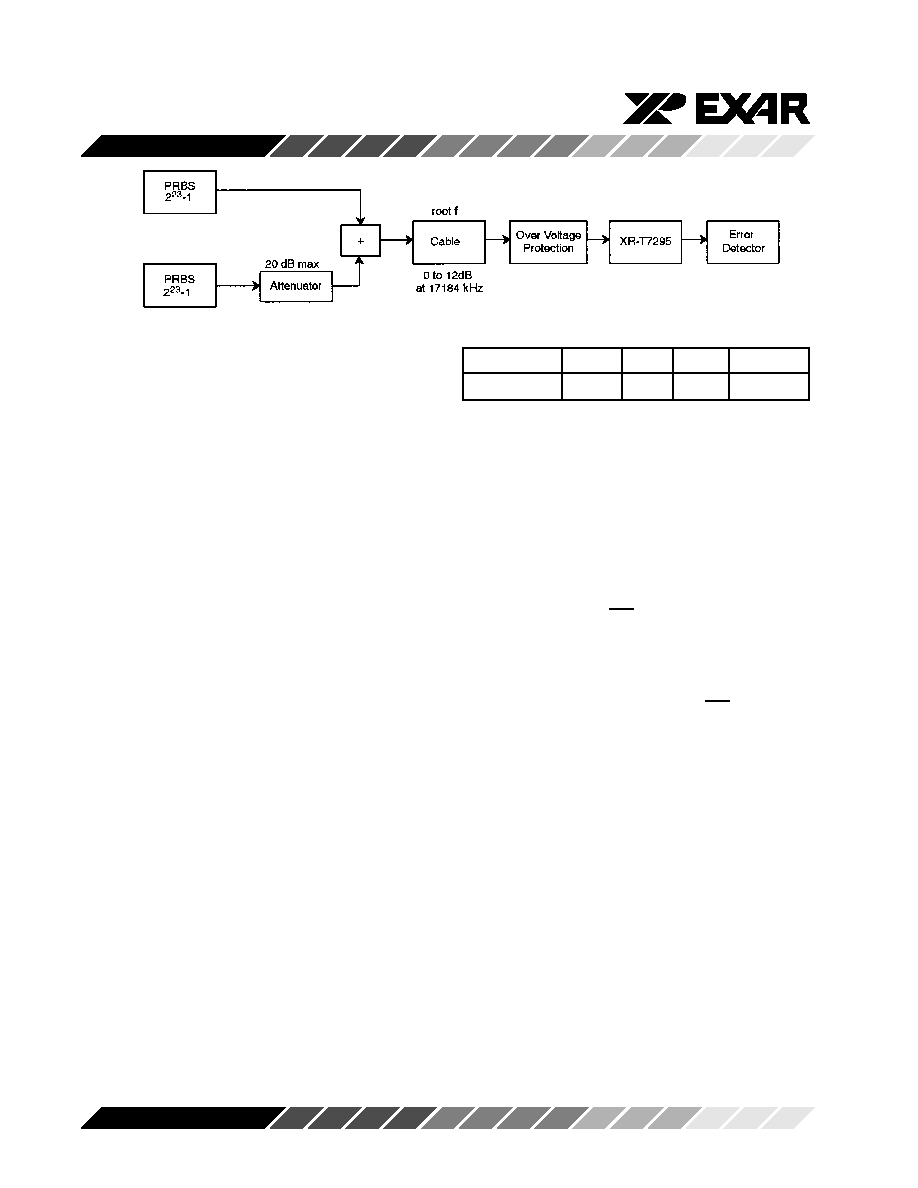
Figure 7. Test Set-up for Interference Immunity Requirements
Digital Detection
In addition to the signal amplitude monitoring of the
analog LOS detector, the digital LOS detector monitors
the recovered data 1s density. The RLOS alarm goes
high if 160 +/-32 or more consecutive bits. The alarm
goes low when at least eight 1s occur in a a string of 32
consecutive bits. This hysteresis minimizes RLOS
chattering and guarantees a minimum RLOS pulse
width of 32 clock cycles.
NOTE:
RLOS chatter can still occur. When REQB=1, input signal
levels above the analog LOS threshold can still be low
enough to result in a high but error rate. The resultant data
stream (containing errors) can temporarily activate the
digital LOS detector, ad RLOS chatter can occur. There-
fore, RLOS should not be used as a bit error rate monitor.
RLOS chatter can also occur when RLOL is activated
(high).
Phase Hits
In response to a 180° phase hit in the input data, the
XRT7295AE returns to error-free operation in less than
2ms. During the reacquisition time, RLOS may be
temporarily indicated.
Recovered Clock and Data Timing
Table 6 and Figure 9 summarize the timing relation-
ships between the high-speed logic signals RCLK,
RPDATA, and RNDATA. All duty cycle and timing
relationships are referenced to V
DD/2 threshold level.
RPDATA and RNDATA change on the rising edge of
RCLK and are valid during the falling edge of RCLK. A
positive pulse at RIN creates a high level on RPDATA
and a low level on RNDATA. A negative pulse creates
a high level on RNDATA and a low level on RPDATA,
and a received zero produces low levels on both
RPDATA and RNDATA.
Table 5. Interference Requirement
Parameter
Min.
Typ.
Max.
Unit
Attenuator
-20
-16
dB
Interference Immunity
The XRT7295AE complies with the interference test
detailed in Figure 7 and Table 5. The two data genera-
tors are non-synchronous.
In-Circuit Test Capability
When pulled low, the ICT pin forces all digital output
buffers (RCLK, RPDATA, RNDATA, RLOS, RLOL
pins) to be placed in a high output impedance state,
This feature allows in-circuit testing to be done on
neighboring devices without concern for XRT7295AE
buffer damage. When forced high, the ICT pin does not
affect device operation. An internal pull-up device
(nominally 50 k
) is provided on this pin; therefore,
users can leave this pin open for normal operation. This
is the only pin for which the internal pull-up/pull-down
is provided.
BOARDLAYOUTCONSIDERATIONS
Power Supply Bypassing
Figure 8 illustrates the recommended power supply
bypassing network. A 0.1
F capacitor bypasses the
digital supplies. The analog supply V
DDA is bypassed
by using a 0.1
F capacitor and a shield bead that
removes significant amounts of high-frequency noise
generated by the system and by the device logic. Good
quality, high-frequency (low lead inductance) capaci-
tors should be used. Finally, it is most important that
all ground connections be made to a low-impedance
ground plane.
相關(guān)PDF資料 |
PDF描述 |
|---|---|
| VE-B64-MX-B1 | CONVERTER MOD DC/DC 48V 75W |
| MS27473T12B35PA | CONN PLUG 22POS STRAIGHT W/PINS |
| MS27468E19F32S | CONN RCPT 32POS JAM NUT W/SCKT |
| IDT72V255LA10TFG8 | IC FIFO SS 8192X18 10NS 64-STQFP |
| MS27467T19A35S | CONN PLUG 66POS STRAIGHT W/SCKT |
相關(guān)代理商/技術(shù)參數(shù) |
參數(shù)描述 |
|---|---|
| XRT7295AEIWTR-F | 功能描述:外圍驅(qū)動器與原件 - PCI E3 Line Receiver RoHS:否 制造商:PLX Technology 工作電源電壓: 最大工作溫度: 安裝風(fēng)格:SMD/SMT 封裝 / 箱體:FCBGA-1156 封裝:Tray |
| XRT7295AT | 制造商:EXAR 制造商全稱:EXAR 功能描述:DS3/Sonet STS-1 Integrated Line Receiver |
| XRT7295AT_10 | 制造商:EXAR 制造商全稱:EXAR 功能描述:DS3 SONET STS1 Integrated Line Receiver |
| XRT7295ATIW | 功能描述:外圍驅(qū)動器與原件 - PCI RoHS:否 制造商:PLX Technology 工作電源電壓: 最大工作溫度: 安裝風(fēng)格:SMD/SMT 封裝 / 箱體:FCBGA-1156 封裝:Tray |
| XRT7295ATIW-F | 功能描述:外圍驅(qū)動器與原件 - PCI -.5V--6.5V temp -45 to 85C RoHS:否 制造商:PLX Technology 工作電源電壓: 最大工作溫度: 安裝風(fēng)格:SMD/SMT 封裝 / 箱體:FCBGA-1156 封裝:Tray |
發(fā)布緊急采購,3分鐘左右您將得到回復(fù)。