- 您現(xiàn)在的位置:買賣IC網(wǎng) > PDF目錄373783 > ZL30120GGG2 (ZARLINK SEMICONDUCTOR INC) SONET/SDH/Ethernet Multi-Rate Line Card Synchronizer PDF資料下載
參數(shù)資料
| 型號: | ZL30120GGG2 |
| 廠商: | ZARLINK SEMICONDUCTOR INC |
| 元件分類: | 數(shù)字傳輸電路 |
| 英文描述: | SONET/SDH/Ethernet Multi-Rate Line Card Synchronizer |
| 中文描述: | ATM/SONET/SDH SUPPORT CIRCUIT, PBGA100 |
| 封裝: | 9 X 9 MM, 0.80 MM PITCH, LEAD FREE, CABGA-100 |
| 文件頁數(shù): | 7/27頁 |
| 文件大小: | 309K |
| 代理商: | ZL30120GGG2 |
第1頁第2頁第3頁第4頁第5頁第6頁當(dāng)前第7頁第8頁第9頁第10頁第11頁第12頁第13頁第14頁第15頁第16頁第17頁第18頁第19頁第20頁第21頁第22頁第23頁第24頁第25頁第26頁第27頁
ZL30120
Data Sheet
7
Zarlink Semiconductor Inc.
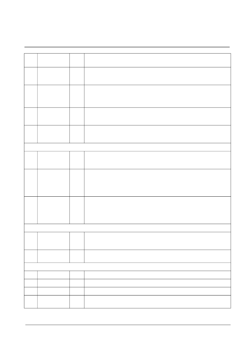
J10
p1_clk0
O
Programmable Synthesizer 1 - Output Clock 0 (LVCMOS).
This output can be
configured to provide any frequency with a multiple of 8 kHz up to 100 MHz in
addition to 2 kHz. The default frequency for this output is 1.544 MHz (DS1).
K10
p1_clk1
O
Programmable Synthesizer1 - Output Clock 1 (LVCMOS).
This is a
programmable clock output configurable as a multiple or division of the p1_clk0
frequency within the range of 2 kHz to 100 MHz. The default frequency for this
output is 3.088 MHz (2x DS1).
H10
fb_clk
O
Feedback Clock (LVCMOS).
This output is a buffered copy of the feedback
clock for DPLL1. The frequency of this output always equals the frequency of the
selected reference.
E1
dpll2_ref
O
DPLL2 Selected Output Reference (LVCMOS).
This is a buffered copy of the
output of the reference selector for DPLL2. Switching between input reference
clocks at this output is not hitless.
Control
H5
rst_b
I
Reset (LVCMOS, Schmitt Trigger).
A logic low at this input resets the device. To
ensure proper operation, the device must be reset after power-up. Reset should
be asserted for a minimum of 300 ns.
J5
dpll1_hs_en
I
u
DPLL1 Hitless Switching Enable (LVCMOS, Schmitt Trigger).
A logic high at
this input enables hitless reference switching. A logic low disables hitless
reference switching and re-aligns DPLL1’s output phase to the phase of the
selected reference input. This feature can also be controlled through software
registers. This pin is internally pulled up to Vdd.
C2
D2
dpll1_mod_sel0
dpll1_mod_sel1
I
u
DPLL1 Mode Select 1:0 (LVCMOS, Schmitt Trigger).
During reset, the levels
on these pins determine the default mode of operation for DPLL1 (Automatic,
Normal, Holdover or Freerun). After reset, the mode of operation can be
controlled directly with these pins, or by accessing the
dpll1_modesel
register
through the serial interface. This pin is internally pulled up to Vdd.
Status
H1
dpll1_lock
O
Lock Indicator (LVCMOS).
This is the lock indicator pin for DPLL1. This output
goes high when DPLL1’s output is frequency and phase locked to the input
reference.
J1
dpll1_holdover
O
Holdover Indicator (LVCMOS).
This pin goes high when DPLL1 enters the
holdover mode.
Serial Interface
E2
sck
I
Clock for Serial Interface (LVCMOS).
Serial interface clock.
F1
si
I
Serial Interface Input (LVCMOS).
Serial interface data input pin.
G1
so
O
Serial Interface Output (LVCMOS).
Serial interface data output pin.
E3
cs_b
I
u
Chip Select for Serial Interface (LVCMOS).
Serial interface chip select. This
pin is internally pulled up to Vdd.
Pin #
Name
I/O
Type
Description
相關(guān)PDF資料 |
PDF描述 |
|---|---|
| ZL30121GGG2 | SONET/SDH Low Jitter System Synchronizer |
| ZL30121 | SONET/SDH Low Jitter System Synchronizer |
| ZL30121GGG | SONET/SDH Low Jitter System Synchronizer |
| ZL30122 | SONET/SDH Low Jitter Line Card Synchronizer |
| ZL30122GGG | SONET/SDH Low Jitter Line Card Synchronizer |
相關(guān)代理商/技術(shù)參數(shù) |
參數(shù)描述 |
|---|---|
| ZL30121 | 制造商:ZARLINK 制造商全稱:Zarlink Semiconductor Inc 功能描述:SONET/SDH Low Jitter System Synchronizer |
| ZL30121GGG | 制造商:Microsemi Corporation 功能描述:SYS SYNCHRONIZER 100CABGA - Trays |
| ZL30121GGG2 | 制造商:Microsemi Corporation 功能描述:PB FREE LOW JITTER SYSTEM SYNCHRONIZER |
| ZL30121GGG2V2 | 制造商:Microsemi Corporation 功能描述:REV 2 PB FREE LOW JITTER SYSTEM SYNCHRO 制造商:Microsemi Corporation 功能描述:REV 2 PB FREE LOW JITTER SYSTEM SYNCHRO - Trays 制造商:MICROSEMI CONSUMER MEDICAL PRODUCT GROUP 功能描述:IC SONET/SDH SYNCH 100CABGA 制造商:Microsemi Corporation 功能描述:IC SONET/SDH SYNCH 100CABGA |
| ZL30121GGGV2 | 制造商:Microsemi Corporation 功能描述:LOW JITTER SYSTEM SYNCHRONIZER 制造商:Microsemi Corporation 功能描述:REV 2 LOW JITTER SYSTEM SYNCHRONIZER - Trays 制造商:MICROSEMI CONSUMER MEDICAL PRODUCT GROUP 功能描述:IC SONET/SDH SYNCH 100CABGA 制造商:Microsemi Corporation 功能描述:IC SONET/SDH SYNCH 100CABGA |
發(fā)布緊急采購,3分鐘左右您將得到回復(fù)。