- 您現(xiàn)在的位置:買賣IC網(wǎng) > PDF目錄1887 > 100-1221-3 (Bluetechnix)CORE MOD CM-BF537E 600MHZ CONN PDF資料下載
參數(shù)資料
| 型號(hào): | 100-1221-3 |
| 廠商: | Bluetechnix |
| 文件頁(yè)數(shù): | 16/68頁(yè) |
| 文件大小: | 0K |
| 描述: | CORE MOD CM-BF537E 600MHZ CONN |
| 標(biāo)準(zhǔn)包裝: | 1 |
| 模塊/板類型: | 核心模塊 |
| 其它名稱: | 100-1221 100-1221-ND |
第1頁(yè)第2頁(yè)第3頁(yè)第4頁(yè)第5頁(yè)第6頁(yè)第7頁(yè)第8頁(yè)第9頁(yè)第10頁(yè)第11頁(yè)第12頁(yè)第13頁(yè)第14頁(yè)第15頁(yè)當(dāng)前第16頁(yè)第17頁(yè)第18頁(yè)第19頁(yè)第20頁(yè)第21頁(yè)第22頁(yè)第23頁(yè)第24頁(yè)第25頁(yè)第26頁(yè)第27頁(yè)第28頁(yè)第29頁(yè)第30頁(yè)第31頁(yè)第32頁(yè)第33頁(yè)第34頁(yè)第35頁(yè)第36頁(yè)第37頁(yè)第38頁(yè)第39頁(yè)第40頁(yè)第41頁(yè)第42頁(yè)第43頁(yè)第44頁(yè)第45頁(yè)第46頁(yè)第47頁(yè)第48頁(yè)第49頁(yè)第50頁(yè)第51頁(yè)第52頁(yè)第53頁(yè)第54頁(yè)第55頁(yè)第56頁(yè)第57頁(yè)第58頁(yè)第59頁(yè)第60頁(yè)第61頁(yè)第62頁(yè)第63頁(yè)第64頁(yè)第65頁(yè)第66頁(yè)第67頁(yè)第68頁(yè)
Rev. J
|
Page 23 of 68
|
February 2014
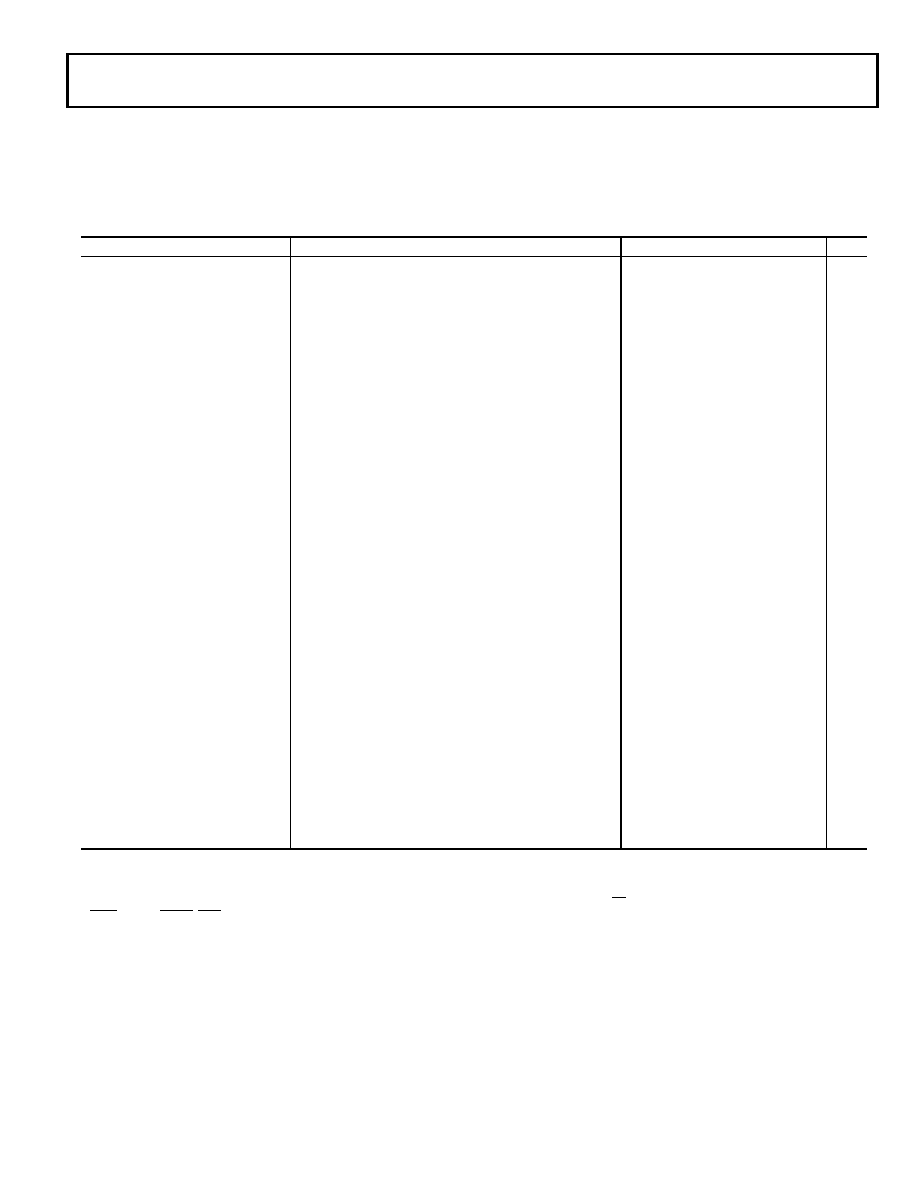
SPECIFICATIONS
Note that component specifications are subject to change
without notice.
OPERATING CONDITIONS
Parameter
Conditions
Min
Nominal
Max
Unit
VDDINT
Internal Supply Voltage1
1 The regulator can generate VDDINT at levels of 0.85 V to 1.2 V with –5% to +10% tolerance, 1.25 V with –4% to +10% tolerance, and 1.3 V with –0% to +10% tolerance. The
required VDDINT is a function of speed grade and operating frequency. See Table 10, Table 11, and Table 12 for details.
Nonautomotive 300 MHz, 400 MHz, and 500 MHz speed
grade models
2
2 See Ordering Guide on Page 67.
0.8
1.2
1.32
V
VDDINT
Internal Supply Voltage1
Nonautomotive 533 MHz speed grade models2
0.8
1.25
1.375
V
VDDINT
Internal Supply Voltage1
Nonautomotive 600 MHz speed grade models2
0.8
1.3
1.43
V
VDDINT
Internal Supply Voltage1
Automotive grade models and +105°C nonautomotive
grade models2
0.95
1.2
1.32
V
VDDEXT
External Supply Voltage
Nonautomotive grade models2
2.25
2.5 or 3.3
3.6
V
VDDEXT
External Supply Voltage
Automotive grade models and +105°C nonautomotive
grade models2
2.7
3.0 or 3.3
3.6
V
VDDRTC
Real-Time Clock Power
Supply Voltage
2.25
3.6
V
VIH
High Level Input Voltage3, 4
3 Bidirectional pins (DATA15–0, PF15–0, PG15–0, PH15–0, TFS0, TSCLK0, RSCLK0, RFS0, MDIO) and input pins (BR, ARDY, DR0PRI, DR0SEC, RTXI, TCK, TDI, TMS,
TRST, CLKIN, RESET, NMI, and BMODE2–0) of the ADSP-BF534/ADSP-BF536/ADSP-BF537 are 3.3 V-tolerant (always accept up to 3.6 V maximum VIH). Voltage
compliance (on outputs, VOH) is limited by the VDDEXT supply voltage.
4 Parameter value applies to all input and bidirectional pins except CLKIN, SDA, and SCL.
VDDEXT = Maximum
2.0
V
VIHCLKIN High Level Input Voltage
5
5 Parameter value applies to CLKIN pin only.
VDDEXT = Maximum
2.2
V
VIH5V
5.0 V Tolerant Pins, High
Level Input Voltage6
6 Applies to pins PJ2/SCL and PJ3/SDA which are 5.0 V tolerant (always accept up to 5.5 V maximum VIH). Voltage compliance (on outputs, VOH) is limited by the VDDEXT supply
voltage.
0.7 × VDDEXT
V
VIH5V
5.0 V Tolerant Pins, High
Level Input Voltage
7
7 Applies to pin PJ4/DR0SEC/CANRX/TACI0 which is 5.0 V tolerant (always accepts up to 5.5 V maximum VIH). Voltage compliance (on outputs, VOH) is limited by the VDDEXT
supply voltage.
VDDEXT = Maximum
2.0
V
VIL
Low Level Input Voltage3, 8
8 Parameter value applies to all input and bidirectional pins except SDA and SCL.
VDDEXT = Minimum
+0.6
V
VIL5V
5.0 V Tolerant Pins, Low
Level Input Voltage
0.3 × VDDEXT V
VIL5V
5.0 V Tolerant Pins, Low
Level Input Voltage
VDDEXT = Minimum
+0.8
V
TJ
Junction Temperature
208-Ball Chip Scale Package Ball Grid Array (CSP_BGA) @
TAMBIENT = –40°C to +105°C
–40
+120
°C
TJ
Junction Temperature
208-Ball Chip Scale Package Ball Grid Array (CSP_BGA) @
TAMBIENT = –40°C to +85°C
–40
+105
°C
TJ
Junction Temperature
208-Ball Chip Scale Package Ball Grid Array (CSP_BGA) @
TAMBIENT = 0°C to +70°C
0+95
°C
TJ
Junction Temperature
182-Ball Chip Scale Package Ball Grid Array (CSP_BGA) @
TAMBIENT = –40°C to +85°C
–40
+105
°C
TJ
Junction Temperature
182-Ball Chip Scale Package Ball Grid Array (CSP_BGA) @
TAMBIENT = 0°C to +70°C
0+100
°C
相關(guān)PDF資料 |
PDF描述 |
|---|---|
| 100-1225-1 | CORE MOD TCM-BF537 500MHZ CONN |
| 100-1254-2 | MODULE BF527-C-C-Q50S64F8 |
| 101-0303 | SMARTSCREEN OP7100 DISPLAY |
| 101-0383 | MODULE RABBITCORE RCM2020 |
| 101-0435 | MODULE RABBITCORE RCM2110 |
相關(guān)代理商/技術(shù)參數(shù) |
參數(shù)描述 |
|---|---|
| 1001224 | 功能描述:防靜電控制產(chǎn)品 12X24 PKG/100 RoHS:否 制造商:3M Electronic Specialty 產(chǎn)品:Air Ionizers 類型:Mini 顏色: 大小:4.5 in x 3.3 in x 2 in |
| 1001225 | 功能描述:防靜電控制產(chǎn)品 12X25 PKG/100 RoHS:否 制造商:3M Electronic Specialty 產(chǎn)品:Air Ionizers 類型:Mini 顏色: 大小:4.5 in x 3.3 in x 2 in |
| 100-1225-1 | 功能描述:CORE MOD TCM-BF537 500MHZ CONN RoHS:是 類別:集成電路 (IC) >> 嵌入式 - 微控制器或微處理器模塊 系列:- 產(chǎn)品目錄繪圖:DLP-245SY-G 標(biāo)準(zhǔn)包裝:1 系列:USB 模塊/板類型:開發(fā)板 適用于相關(guān)產(chǎn)品:USB 其它名稱:813-1006 |
| 10-01-2259 | 功能描述:集管和線殼 KK 100 Housing Crimp Crimp Std 25 Ckt RoHS:否 產(chǎn)品種類:1.0MM Rectangular Connectors 產(chǎn)品類型:Headers - Pin Strip 系列:DF50 觸點(diǎn)類型:Pin (Male) 節(jié)距:1 mm 位置/觸點(diǎn)數(shù)量:16 排數(shù):1 安裝風(fēng)格:SMD/SMT 安裝角:Right 端接類型:Solder 外殼材料:Liquid Crystal Polymer (LCP) 觸點(diǎn)材料:Brass 觸點(diǎn)電鍍:Gold 制造商:Hirose Connector |
| 100122A | 制造商:未知廠家 制造商全稱:未知廠家 功能描述:Nine Bit Buffer |
發(fā)布緊急采購(gòu),3分鐘左右您將得到回復(fù)。