- 您現(xiàn)在的位置:買賣IC網(wǎng) > PDF目錄371406 > 25AA1024 (Microchip Technology Inc.) 1 Mbit SPI Bus Serial EEPROM PDF資料下載
參數(shù)資料
| 型號: | 25AA1024 |
| 廠商: | Microchip Technology Inc. |
| 英文描述: | 1 Mbit SPI Bus Serial EEPROM |
| 中文描述: | 1兆位SPI總線串行EEPROM |
| 文件頁數(shù): | 12/30頁 |
| 文件大?。?/td> | 459K |
| 代理商: | 25AA1024 |
第1頁第2頁第3頁第4頁第5頁第6頁第7頁第8頁第9頁第10頁第11頁當前第12頁第13頁第14頁第15頁第16頁第17頁第18頁第19頁第20頁第21頁第22頁第23頁第24頁第25頁第26頁第27頁第28頁第29頁第30頁

25AA1024/25LC1024
DS21836D-page 12
Preliminary
2007 Microchip Technology Inc.
2.5
Write Status Register Instruction
(
WRSR
)
The Write Status Register instruction (
WRSR
) allows the
user to write to the nonvolatile bits in the STATUS
register as shown in Table 2-2. The user is able to
select one of four levels of protection for the array by
writing to the appropriate bits in the STATUS register.
The array is divided up into four segments. The user
has the ability to write-protect none, one, two, or all four
of the segments of the array. The partitioning is
controlled as shown in Table 2-3.
The Write-Protect Enable (WPEN) bit is a nonvolatile
bit that is available as an enable bit for the WP pin. The
Write-Protect (WP) pin and the Write-Protect Enable
(WPEN) bit in the STATUS register control the
programmable hardware write-protect feature. Hard-
ware write protection is enabled when WP pin is low
and the WPEN bit is high. Hardware write protection is
disabled when either the WP pin is high or the WPEN
bit is low. When the chip is hardware write-protected,
only writes to nonvolatile bits in the STATUS register
are disabled. See Table 2-4 for a matrix of functionality
on the WPEN bit.
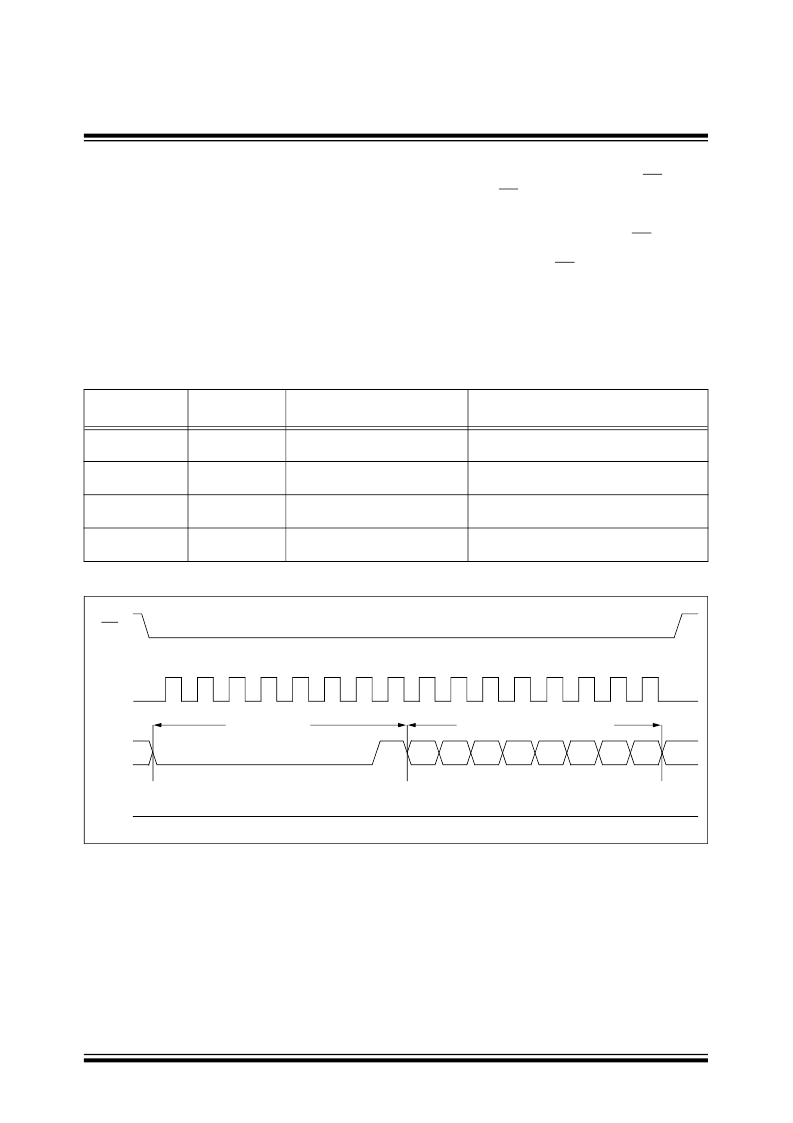
See Figure 2-7 for the WRSR timing sequence.
TABLE 2-3:
ARRAY PROTECTION
FIGURE 2-7:
WRITE STATUS REGISTER TIMING SEQUENCE (
WRSR
)
BP1
BP0
Array Addresses
Write-Protected
Array Addresses
Unprotected
0
0
none
All (Sectors 0, 1, 2 & 3)
(00000h-1FFFFh)
Lower 3/4 (Sectors 0, 1 & 2)
(00000h-17FFFh)
Lower 1/2 (Sectors 0 & 1)
(00000h-0FFFFh)
none
0
1
Upper 1/4 (Sector 3)
(18000h-1FFFFh)
Upper 1/2 (Sectors 2 & 3)
(10000h-1FFFFh)
All (Sectors 0, 1, 2 & 3)
(00000h-1FFFFh)
1
0
1
1
SO
SI
CS
9
10
11
12
13
14
15
0
1
0
0
0
0
0
0
7
6
5
4
2
1
0
Instruction
Data to STATUS register
High-Impedance
SCK
0
2
3
4
5
6
7
1
8
3
相關PDF資料 |
PDF描述 |
|---|---|
| 25AA128 | 128K SPI Bus Serial EEPROM |
| 25AA160A | 16K SPI Bus Serial EEPROM |
| 25AA160B | PHOTOTRANSISTOR NPN 890NM TO-18 |
| 25LC160A | 16K SPI Bus Serial EEPROM |
| 25AA320A_07 | 32K SPI Bus Serial EEPROM |
相關代理商/技術參數(shù) |
參數(shù)描述 |
|---|---|
| 25AA1024_10 | 制造商:MICROCHIP 制造商全稱:Microchip Technology 功能描述:1 Mbit SPI Bus Serial EEPROM |
| 25AA1024_1005 | 制造商:MICROCHIP 制造商全稱:Microchip Technology 功能描述:1 Mbit SPI Bus Serial EEPROM |
| 25AA1024-E/MF | 制造商:MICROCHIP 制造商全稱:Microchip Technology 功能描述:1 Mbit SPI Bus Serial EEPROM |
| 25AA1024-E/P | 制造商:MICROCHIP 制造商全稱:Microchip Technology 功能描述:1 Mbit SPI Bus Serial EEPROM |
| 25AA1024-E/SM | 制造商:MICROCHIP 制造商全稱:Microchip Technology 功能描述:1 Mbit SPI Bus Serial EEPROM |
發(fā)布緊急采購,3分鐘左右您將得到回復。