- 您現(xiàn)在的位置:買賣IC網(wǎng) > PDF目錄222810 > 70T3399S133BCGI8 (INTEGRATED DEVICE TECHNOLOGY INC) 128K X 18 DUAL-PORT SRAM, 15 ns, PBGA256 PDF資料下載
參數(shù)資料
| 型號: | 70T3399S133BCGI8 |
| 廠商: | INTEGRATED DEVICE TECHNOLOGY INC |
| 元件分類: | SRAM |
| 英文描述: | 128K X 18 DUAL-PORT SRAM, 15 ns, PBGA256 |
| 封裝: | 17 X 17 MM, 1.40 MM HEIGHT, 1 MM PITCH, BGA-256 |
| 文件頁數(shù): | 14/28頁 |
| 文件大?。?/td> | 327K |
| 代理商: | 70T3399S133BCGI8 |
第1頁第2頁第3頁第4頁第5頁第6頁第7頁第8頁第9頁第10頁第11頁第12頁第13頁當前第14頁第15頁第16頁第17頁第18頁第19頁第20頁第21頁第22頁第23頁第24頁第25頁第26頁第27頁第28頁
6.42
IDT70T3339/19/99S
High-Speed 2.5V 512/256/128K x 18 Dual-Port Static RAM
Industrial and Commercial Temperature Ranges
21
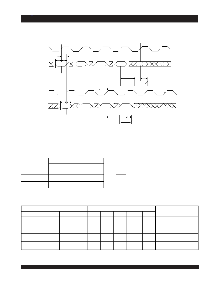
tSA
tHA
(3)
tCOLS
tCOLR
A3
HA
tSA
t
tCOLS
tCOLR
5652 drw 20
COLR
COLL
(4)
CLKR
ADDRESSR
A0
A1
A2
tOFS
(4)
CLKL
ADDRESSL
A0
A1
A2
A3
tOFS
Waveform of Collision Timing (1,2)
Both Ports Writing with Left Port Clock Leading
Collision Detection Timing(3,4)
Cycle Time
tOFS (ns)
Region 1 (ns) (1)
Region 2 (ns) (2)
5ns
0 - 2.8
2.81 - 4.6
6ns
0 - 3.8
3.81 - 5.6
7.5ns
0 - 5.3
5.31 - 7.1
5652 tb l 13
NOTES:
1. Region 1
Both ports show collision after 2nd cycle for Addresses 0, 2, 4 etc.
2. Region 2
Leading port shows collision after 3rd cycle for addresses 0, 3, 6, etc.
while trailing port shows collision after 2nd cycle for addresses 0, 2, 4 etc.
3. All the production units are tested to midpoint of each region.
4. These ranges are based on characterization of a typical device.
Left Port
Right Port
Function
CLKL
R/
WL(1)
CEL
(1)
A18L-A0L
(2)
COLL
CLKR
R/
WR(1)
CER
(1)
A18R-A0R
(2)
COLR
↑
HL
MATCH
H
↑
HL
MATCH
H
Both ports reading. Not a valid collision.
No flag output on either port.
↑
HL
MATCH
L
↑
LL
MATCH
H
Left port reading, Right port writing.
Valid collision, flag output on Left port.
↑
LL
MATCH
H
↑
HL
MATCH
L
Right port reading, Left port writing.
Valid collision, flag output on Right port.
↑
LL
MATCH
L
↑
LL
MATCH
L
Both ports writing. Valid collision. Flag
output on both ports.
5652 tbl 14
Truth Table IV — Collision Detection Flag
NOTES:
1.
CE0 = VIL and CE1 = VIH. R/W and CE are synchronous with respect to the clock and need valid set-up and hold times.
2. Address is for internal register, not the external bus, i.e., address needs to be qualified by one of the Address counter control signals.
NOTES:
1.
CE0 = VIL, CE1 = VIH.
2. For reading port,
OE is a Don't care on the Collision Detection Logic. Please refer to Truth Table IV for specific cases.
3. Leading Port Output flag might output 3tCYC2 + tCOLS after Address match.
4. Address is for internal register, not the external bus, i.e., address needs to be qualified by one of the Address counter control signals.
相關(guān)PDF資料 |
PDF描述 |
|---|---|
| 70TPS12 | 75 A, 1200 V, SCR, TO-274AA |
| 70TPS16 | 75 A, 1600 V, SCR, TO-274AA |
| 70TPS12PBF | 75 A, 1200 V, SCR, TO-274AA |
| 70TPS16PBF | 75 A, 1600 V, SCR, TO-274AA |
| 70V657S12BFG8 | 32K X 36 DUAL-PORT SRAM, 12 ns, PBGA208 |
相關(guān)代理商/技術(shù)參數(shù) |
參數(shù)描述 |
|---|---|
| 70T3399S133BCI | 制造商:Integrated Device Technology Inc 功能描述:SRAM Chip Sync Dual 2.5V 2M-Bit 128K x 18 15ns/4.2ns 256-Pin CABGA Tray 制造商:Integrated Device Technology Inc 功能描述:SRAM SYNC DUAL 2.5V 2.25MBIT 128KX18 15NS/4.2NS 256BGA - Rail/Tube |
| 70T3399S133BCI8 | 制造商:Integrated Device Technology Inc 功能描述:SRAM Chip Sync Dual 2.5V 2M-Bit 128K x 18 15ns/4.2ns 256-Pin CABGA T/R 制造商:Integrated Device Technology Inc 功能描述:SRAM SYNC DUAL 2.5V 2.25MBIT 128KX18 15NS/4.2NS 256BGA - Tape and Reel |
| 70T3399S133BF | 制造商:Integrated Device Technology Inc 功能描述:SRAM Chip Sync Dual 2.5V 2M-Bit 128K x 18 15ns/4.2ns 208-Pin CABGA Tray 制造商:Integrated Device Technology Inc 功能描述:SRAM SYNC DUAL 2.5V 2.25MBIT 128KX18 15NS/4.2NS 208FPBGA - Rail/Tube |
| 70T3399S133BF8 | 制造商:Integrated Device Technology Inc 功能描述:SRAM Chip Sync Dual 2.5V 2M-Bit 128K x 18 15ns/4.2ns 208-Pin CABGA T/R 制造商:Integrated Device Technology Inc 功能描述:SRAM SYNC DUAL 2.5V 2.25MBIT 128KX18 15NS/4.2NS 208FPBGA - Tape and Reel |
| 70T3399S133BFI | 制造商:Integrated Device Technology Inc 功能描述:SRAM Chip Sync Dual 2.5V 2M-Bit 128K x 18 15ns/4.2ns 208-Pin CABGA Tray 制造商:Integrated Device Technology Inc 功能描述:SRAM SYNC DUAL 2.5V 2.25MBIT 128KX18 15NS/4.2NS 208FPBGA - Rail/Tube |
發(fā)布緊急采購,3分鐘左右您將得到回復(fù)。