- 您現(xiàn)在的位置:買賣IC網(wǎng) > PDF目錄352476 > A42MX16-1PL100M (Electronic Theatre Controls, Inc.) IC TVS BI-DIR 24V 350W SOD-323 PDF資料下載
參數(shù)資料
| 型號: | A42MX16-1PL100M |
| 廠商: | Electronic Theatre Controls, Inc. |
| 英文描述: | IC TVS BI-DIR 24V 350W SOD-323 |
| 中文描述: | 40MX和42MX FPGA系列 |
| 文件頁數(shù): | 106/120頁 |
| 文件大小: | 854K |
| 代理商: | A42MX16-1PL100M |
第1頁第2頁第3頁第4頁第5頁第6頁第7頁第8頁第9頁第10頁第11頁第12頁第13頁第14頁第15頁第16頁第17頁第18頁第19頁第20頁第21頁第22頁第23頁第24頁第25頁第26頁第27頁第28頁第29頁第30頁第31頁第32頁第33頁第34頁第35頁第36頁第37頁第38頁第39頁第40頁第41頁第42頁第43頁第44頁第45頁第46頁第47頁第48頁第49頁第50頁第51頁第52頁第53頁第54頁第55頁第56頁第57頁第58頁第59頁第60頁第61頁第62頁第63頁第64頁第65頁第66頁第67頁第68頁第69頁第70頁第71頁第72頁第73頁第74頁第75頁第76頁第77頁第78頁第79頁第80頁第81頁第82頁第83頁第84頁第85頁第86頁第87頁第88頁第89頁第90頁第91頁第92頁第93頁第94頁第95頁第96頁第97頁第98頁第99頁第100頁第101頁第102頁第103頁第104頁第105頁當前第106頁第107頁第108頁第109頁第110頁第111頁第112頁第113頁第114頁第115頁第116頁第117頁第118頁第119頁第120頁
86
4958B–AUTO–11/10
Atmel ATA6285/ATA6286 [Preliminary]
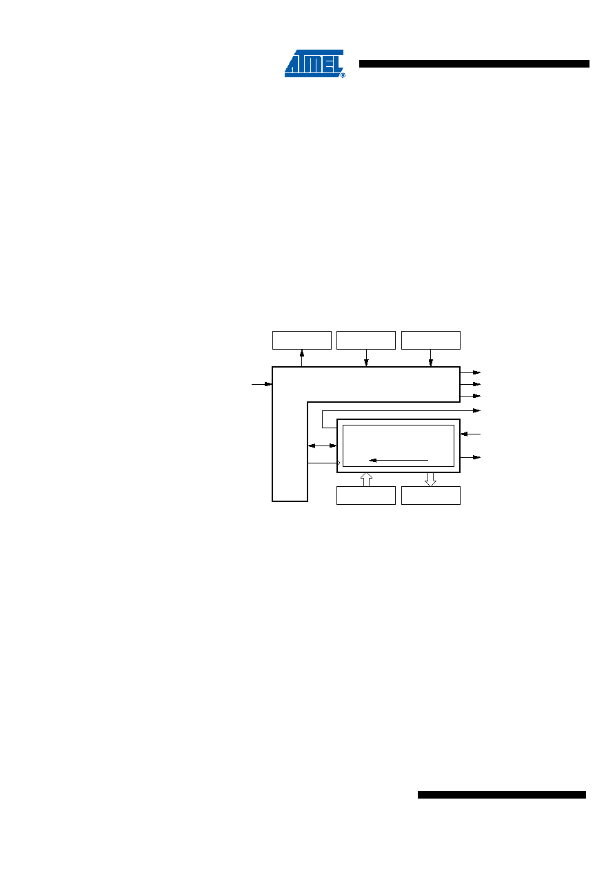
3.13.5.5
Modulator Synchronous Serial Interface (SSI)
The Synchronous Serial Interface (SSI) allows synchronous data transfer between the ATA6289
and the peripheral devices and also the generation of Biphase code, Manchester code or PWM
code together with the serial data output into a continuous serial stream of data. The SSI consist
a 8-bit shift register (SR), a SSI I/O data register (T2MDR), a mode register (T2MRB), a status
register (T2IFR), an interrupt mask register (T2IMR), an input clock (CLK
T2), two serial data I/O
lines (SI and SO), a shift clock I/O line (SCLK) and three different interrupt request signals
(T2RXB, T2TXB, T2TXC). The Figure 3-34 shows the Synchronous Serial Interface (SSI).
The SSI includes following features:
Full-duplex, Three-wire Synchronous Data Transfer
Only Master Operation
MSB First Data Transfer
Generation of a Continuous Serial Stream of Data
End of Transmission Interrupt Flag
Figure 3-34. Synchronous Serial Interface (SSI)
The SSI contains a 8-bit shift register with two associated 8-bit buffers - the receive buffer
T2MDR (RXD) to capture incoming serial data and a transmit buffer T2MDR (TXD) to store the
data for the serial data output. Both buffers share the same I/O addresses labeled as Timer2
Modulator Data Register or T2MDR and can be directly accessed by software. The SSI automat-
ically controls the data transfer between transmit and receive buffer and the 8-Bit shift register.
In that way either single byte transfers or continuous bit streams can be supported.
The SSI is always master. The required clock for the data interchange is accessible on the
SCLK line from the Timer2/counter2 stage output clock (CLK
T2). SCLK is half the clock of CLKT2.
With this additional division by 2 we ensure a duty cycle of 50% for SCLK which is important for
the SSI data transfer (see Figure 3-36 on page 93). The data is always shifted from Master to
Slave on the Serial data Output line (SO), and from Slave to Master on the serial data Input line
(SI). Serial data is organized in 8-bit telegrams which are shifted with the most significant bit
(MSB) first.
T2IFR
T2IMR
MSB
T2RXB
T2TXB
SCLK
CLKT2
SI
SO
T2TXC
LSB
8-Bit Shift Register (SR)
SSI-Control
T2MRB
T2MDR(TXD)
T2MDR(RXD)
相關PDF資料 |
PDF描述 |
|---|---|
| A42MX02-1BG100 | 40MX and 42MX FPGA Families |
| A42MX04-1BG100 | 40MX and 42MX FPGA Families |
| A42MX09-1BG100 | 40MX and 42MX FPGA Families |
| A42MX24-1BG100 | 40MX and 42MX FPGA Families |
| A42MX02-1CQ100ES | 40MX and 42MX FPGA Families |
相關代理商/技術參數(shù) |
參數(shù)描述 |
|---|---|
| A42MX16-1PL84 | 功能描述:IC FPGA MX SGL CHIP 24K 84-PLCC RoHS:否 類別:集成電路 (IC) >> 嵌入式 - FPGA(現(xiàn)場可編程門陣列) 系列:MX 標準包裝:40 系列:SX-A LAB/CLB數(shù):6036 邏輯元件/單元數(shù):- RAM 位總計:- 輸入/輸出數(shù):360 門數(shù):108000 電源電壓:2.25 V ~ 5.25 V 安裝類型:表面貼裝 工作溫度:0°C ~ 70°C 封裝/外殼:484-BGA 供應商設備封裝:484-FPBGA(27X27) |
| A42MX16-1PL84I | 功能描述:IC FPGA MX SGL CHIP 24K 84-PLCC RoHS:否 類別:集成電路 (IC) >> 嵌入式 - FPGA(現(xiàn)場可編程門陣列) 系列:MX 標準包裝:40 系列:SX-A LAB/CLB數(shù):6036 邏輯元件/單元數(shù):- RAM 位總計:- 輸入/輸出數(shù):360 門數(shù):108000 電源電壓:2.25 V ~ 5.25 V 安裝類型:表面貼裝 工作溫度:0°C ~ 70°C 封裝/外殼:484-BGA 供應商設備封裝:484-FPBGA(27X27) |
| A42MX16-1PL84M | 制造商:Microsemi Corporation 功能描述:FPGA 42MX Family 24K Gates 608 Cells 119MHz/198MHz 0.45um Technology 3.3V/5V 84-Pin PLCC 制造商:Microsemi Corporation 功能描述:FPGA 24K GATES 608 CELLS 119MHZ/198MHZ 0.45UM 3.3V/5V 84PLCC - Rail/Tube 制造商:Microsemi Corporation 功能描述:IC FPGA 72 I/O 84PLCC 制造商:Microsemi Corporation 功能描述:IC FPGA MX SGL CHIP 24K 84-PLCC |
| A42MX16-1PLG84 | 功能描述:IC FPGA MX SGL CHIP 24K 84-PLCC RoHS:是 類別:集成電路 (IC) >> 嵌入式 - FPGA(現(xiàn)場可編程門陣列) 系列:MX 標準包裝:40 系列:SX-A LAB/CLB數(shù):6036 邏輯元件/單元數(shù):- RAM 位總計:- 輸入/輸出數(shù):360 門數(shù):108000 電源電壓:2.25 V ~ 5.25 V 安裝類型:表面貼裝 工作溫度:0°C ~ 70°C 封裝/外殼:484-BGA 供應商設備封裝:484-FPBGA(27X27) |
| A42MX16-1PLG84I | 功能描述:IC FPGA MX SGL CHIP 24K 84-PLCC RoHS:是 類別:集成電路 (IC) >> 嵌入式 - FPGA(現(xiàn)場可編程門陣列) 系列:MX 標準包裝:40 系列:SX-A LAB/CLB數(shù):6036 邏輯元件/單元數(shù):- RAM 位總計:- 輸入/輸出數(shù):360 門數(shù):108000 電源電壓:2.25 V ~ 5.25 V 安裝類型:表面貼裝 工作溫度:0°C ~ 70°C 封裝/外殼:484-BGA 供應商設備封裝:484-FPBGA(27X27) |
發(fā)布緊急采購,3分鐘左右您將得到回復。