- 您現(xiàn)在的位置:買賣IC網(wǎng) > PDF目錄352476 > A42MX16-1PL100M (Electronic Theatre Controls, Inc.) IC TVS BI-DIR 24V 350W SOD-323 PDF資料下載
參數(shù)資料
| 型號(hào): | A42MX16-1PL100M |
| 廠商: | Electronic Theatre Controls, Inc. |
| 英文描述: | IC TVS BI-DIR 24V 350W SOD-323 |
| 中文描述: | 40MX和42MX FPGA系列 |
| 文件頁數(shù): | 21/120頁 |
| 文件大小: | 854K |
| 代理商: | A42MX16-1PL100M |
第1頁第2頁第3頁第4頁第5頁第6頁第7頁第8頁第9頁第10頁第11頁第12頁第13頁第14頁第15頁第16頁第17頁第18頁第19頁第20頁當(dāng)前第21頁第22頁第23頁第24頁第25頁第26頁第27頁第28頁第29頁第30頁第31頁第32頁第33頁第34頁第35頁第36頁第37頁第38頁第39頁第40頁第41頁第42頁第43頁第44頁第45頁第46頁第47頁第48頁第49頁第50頁第51頁第52頁第53頁第54頁第55頁第56頁第57頁第58頁第59頁第60頁第61頁第62頁第63頁第64頁第65頁第66頁第67頁第68頁第69頁第70頁第71頁第72頁第73頁第74頁第75頁第76頁第77頁第78頁第79頁第80頁第81頁第82頁第83頁第84頁第85頁第86頁第87頁第88頁第89頁第90頁第91頁第92頁第93頁第94頁第95頁第96頁第97頁第98頁第99頁第100頁第101頁第102頁第103頁第104頁第105頁第106頁第107頁第108頁第109頁第110頁第111頁第112頁第113頁第114頁第115頁第116頁第117頁第118頁第119頁第120頁
117
4958B–AUTO–11/10
Atmel ATA6285/ATA6286 [Preliminary]
3.14.1.5
SPI Data Register – SPDR
The SPI Data Register is a read/write register used for data transfer between the Register File
and the SPI Shift Register. Writing to the register initiates data transmission. Reading the regis-
ter causes the Shift Register Receive buffer to be read.
3.14.2
Data Modes
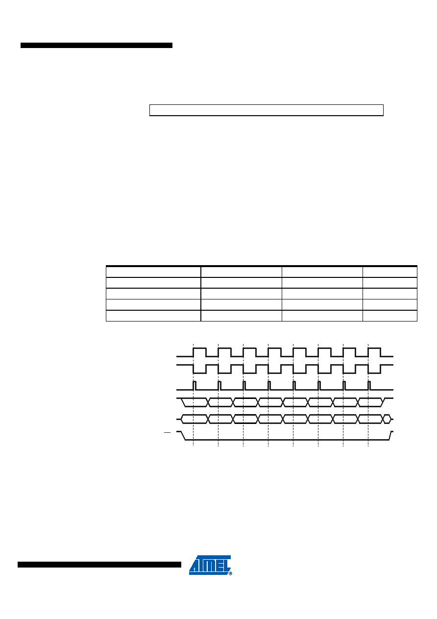
There are four combinations of SCK phase and polarity with respect to serial data, which are
determined by control bits CPHA and CPOL. The SPI data transfer formats are shown in Figure
3-54 and Figure 3-55 on page 118. Data bits are shifted out and latched in on opposite edges of
the SCK signal, ensuring sufficient time for data signals to stabilize. This is clearly seen by sum-
Figure 3-54. SPI Transfer Format with CPHA = 0
Bit
765
432
10
SPDR[7..0]
SPDR
Read/Write
R/W
Initial Value
X
XXX
X
Undefined
Table 3-50.
CPOL/CHPA Functionality
Leading Edge
Trailing Edge
SPI Mode
CPOL = 0, CPHA = 0
Sample(Rising)
Setup(Falling)
0
CPOL = 0, CPHA = 1
Setup(Rising)
Sample(Falling)
1
CPOL = 1, CPHA = 0
Sample(Falling)
Setup(Rising)
2
CPOL = 1, CPHA = 1
Setup(Falling)
Sample(Rising)
3
LSB
MSB
Bit 1
Bit 6
Bit 2
Bit 5
Bit 3
Bit 4
Bit 3
Bit 5
Bit 2
Bit 6
Bit 1
MSB
LSB
MSB first (DORD = 0)
LSB first (DORD =1)
SCK (CPOL = 0)
mode 0
SCK (CPOL = 1)
mode 2
SS
SAMPLE -
MOSI/MISO
MISO - PIN
MOSI - PIN
相關(guān)PDF資料 |
PDF描述 |
|---|---|
| A42MX02-1BG100 | 40MX and 42MX FPGA Families |
| A42MX04-1BG100 | 40MX and 42MX FPGA Families |
| A42MX09-1BG100 | 40MX and 42MX FPGA Families |
| A42MX24-1BG100 | 40MX and 42MX FPGA Families |
| A42MX02-1CQ100ES | 40MX and 42MX FPGA Families |
相關(guān)代理商/技術(shù)參數(shù) |
參數(shù)描述 |
|---|---|
| A42MX16-1PL84 | 功能描述:IC FPGA MX SGL CHIP 24K 84-PLCC RoHS:否 類別:集成電路 (IC) >> 嵌入式 - FPGA(現(xiàn)場(chǎng)可編程門陣列) 系列:MX 標(biāo)準(zhǔn)包裝:40 系列:SX-A LAB/CLB數(shù):6036 邏輯元件/單元數(shù):- RAM 位總計(jì):- 輸入/輸出數(shù):360 門數(shù):108000 電源電壓:2.25 V ~ 5.25 V 安裝類型:表面貼裝 工作溫度:0°C ~ 70°C 封裝/外殼:484-BGA 供應(yīng)商設(shè)備封裝:484-FPBGA(27X27) |
| A42MX16-1PL84I | 功能描述:IC FPGA MX SGL CHIP 24K 84-PLCC RoHS:否 類別:集成電路 (IC) >> 嵌入式 - FPGA(現(xiàn)場(chǎng)可編程門陣列) 系列:MX 標(biāo)準(zhǔn)包裝:40 系列:SX-A LAB/CLB數(shù):6036 邏輯元件/單元數(shù):- RAM 位總計(jì):- 輸入/輸出數(shù):360 門數(shù):108000 電源電壓:2.25 V ~ 5.25 V 安裝類型:表面貼裝 工作溫度:0°C ~ 70°C 封裝/外殼:484-BGA 供應(yīng)商設(shè)備封裝:484-FPBGA(27X27) |
| A42MX16-1PL84M | 制造商:Microsemi Corporation 功能描述:FPGA 42MX Family 24K Gates 608 Cells 119MHz/198MHz 0.45um Technology 3.3V/5V 84-Pin PLCC 制造商:Microsemi Corporation 功能描述:FPGA 24K GATES 608 CELLS 119MHZ/198MHZ 0.45UM 3.3V/5V 84PLCC - Rail/Tube 制造商:Microsemi Corporation 功能描述:IC FPGA 72 I/O 84PLCC 制造商:Microsemi Corporation 功能描述:IC FPGA MX SGL CHIP 24K 84-PLCC |
| A42MX16-1PLG84 | 功能描述:IC FPGA MX SGL CHIP 24K 84-PLCC RoHS:是 類別:集成電路 (IC) >> 嵌入式 - FPGA(現(xiàn)場(chǎng)可編程門陣列) 系列:MX 標(biāo)準(zhǔn)包裝:40 系列:SX-A LAB/CLB數(shù):6036 邏輯元件/單元數(shù):- RAM 位總計(jì):- 輸入/輸出數(shù):360 門數(shù):108000 電源電壓:2.25 V ~ 5.25 V 安裝類型:表面貼裝 工作溫度:0°C ~ 70°C 封裝/外殼:484-BGA 供應(yīng)商設(shè)備封裝:484-FPBGA(27X27) |
| A42MX16-1PLG84I | 功能描述:IC FPGA MX SGL CHIP 24K 84-PLCC RoHS:是 類別:集成電路 (IC) >> 嵌入式 - FPGA(現(xiàn)場(chǎng)可編程門陣列) 系列:MX 標(biāo)準(zhǔn)包裝:40 系列:SX-A LAB/CLB數(shù):6036 邏輯元件/單元數(shù):- RAM 位總計(jì):- 輸入/輸出數(shù):360 門數(shù):108000 電源電壓:2.25 V ~ 5.25 V 安裝類型:表面貼裝 工作溫度:0°C ~ 70°C 封裝/外殼:484-BGA 供應(yīng)商設(shè)備封裝:484-FPBGA(27X27) |
發(fā)布緊急采購,3分鐘左右您將得到回復(fù)。