- 您現(xiàn)在的位置:買賣IC網(wǎng) > PDF目錄362031 > A54SX08AFG144M Logic IC PDF資料下載
參數(shù)資料
| 型號(hào): | A54SX08AFG144M |
| 英文描述: | Logic IC |
| 中文描述: | 邏輯IC |
| 文件頁數(shù): | 9/36頁 |
| 文件大小: | 833K |
| 代理商: | A54SX08AFG144M |
第1頁第2頁第3頁第4頁第5頁第6頁第7頁第8頁當(dāng)前第9頁第10頁第11頁第12頁第13頁第14頁第15頁第16頁第17頁第18頁第19頁第20頁第21頁第22頁第23頁第24頁第25頁第26頁第27頁第28頁第29頁第30頁第31頁第32頁第33頁第34頁第35頁第36頁
v2.0
9
54SX Family FPGAs RadTolerant and HiRel
Boundary Scan Testing (BST)
All RT54SX devices are IEEE 1149.1 (JTAG) compliant.
They offer superior diagnostic and testing capabilities by
providing Boundary Scan Testing (BST) and probing
capabilities. These functions are controlled through the
special test pins in conjunction with the program fuse. The
functionality of each pin is described in
Table 2
.
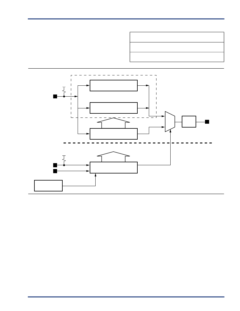
Figure 10
is a block diagram of the RT54SX JTAG circuitry.
Configuring Diagnostic Pins
The JTAG and Probe pins (TDI, TCK, TMS, TDO, PRA, and
PRB) are placed in the desired mode by selecting the
appropriate check boxes in the
“
Variation
”
dialog window.
This dialog window is accessible through the Design Setup
Wizard under the Tools menu in Actel
’
s Designer software.
TRST pin
The TRST pin functions as a Boundary Scan Reset pin. The
TRST pin is an asynchronous, active-low input to initialize
or reset the BST circuit. An internal pull-up resistor is
automatically enabled on the TRST pin.
Dedicated Test Mode
When the
“
Reserve JTAG
”
box is checked in the Designer
software, the RT54SX is placed in Dedicated Test mode, which
configures the TDI, TCK, and TDO pins for BST or in-circuit
verification with Silicon Explorer II. An internal pull-up resistor
is automatically enabled on both the TMS and TDI pins. In
dedicated test mode, TCK, TDI, and TDO are dedicated test pins
and become unavailable for pin assignment in the Pin Editor.
The TMS pin will function as specified in the IEEE 1149.1
(JTAG) Specification.
Flexible Mode
When the
“
Reserve JTAG
”
box is not selected (default setting
in Designer software), the RT54SX is placed in flexible mode,
which allows the TDI, TCK, and TDO pins to function as user
I/Os or BST pins. In this mode the internal pull-up resistors on
the TMS and TDI pins are disabled. An external 10k
pull-up
resistor to VCCI is required on the TMS pin.
The TDI, TCK, and TDO pins are transformed from user I/Os
into BST pins when a rising edge on TCK is detected while
TMS is at logical low. Once the BST pins are in test mode
they will remain in BST mode until the internal BST state
Table 2
Boundary Scan Pin Functionality
Program Fuse Blown
(Dedicated Test Mode)
Program Fuse Not Blown
(Flexible Mode)
TCK, TDI, TDO are
dedicated test pins
No need for pull-up resistor
for TMS
TCK, TDI, TDO are flexible
and may be used as I/Os
Use a pull-up resistor of
10k
on TMS
Figure 10
RT54SX JTAG Circuitry
Instruction Register (IR)
Data Registers (DRs)
clocks and/or controls
TAP Controller
output
stage
0
1
TDO
TDI
TMS
TCK
TRST external
hard-wired pin
相關(guān)PDF資料 |
PDF描述 |
|---|---|
| A54SX08-FG144 | Field Programmable Gate Array (FPGA) |
| A54SX08-FG144I | Field Programmable Gate Array (FPGA) |
| A54SX08-PL84 | Field Programmable Gate Array (FPGA) |
| A54SX08-PL84I | Field Programmable Gate Array (FPGA) |
| A54SX08-PL84M | Field Programmable Gate Array (FPGA) |
相關(guān)代理商/技術(shù)參數(shù) |
參數(shù)描述 |
|---|---|
| A54SX08A-FG208 | 制造商:未知廠家 制造商全稱:未知廠家 功能描述:SX-A Family FPGAs |
| A54SX08AFG208A | 制造商:ACTEL 制造商全稱:Actel Corporation 功能描述:SX-A Family FPGAs |
| A54SX08A-FG208A | 制造商:未知廠家 制造商全稱:未知廠家 功能描述:SX-A Family FPGAs |
| A54SX08A-FG208B | 制造商:未知廠家 制造商全稱:未知廠家 功能描述:SX-A Family FPGAs |
| A54SX08AFG208I | 制造商:ACTEL 制造商全稱:Actel Corporation 功能描述:SX-A Family FPGAs |
發(fā)布緊急采購,3分鐘左右您將得到回復(fù)。