- 您現(xiàn)在的位置:買賣IC網(wǎng) > PDF目錄366329 > ACE9030 (Mitel Networks Corporation) Radio Interface and Twin Synthesiser(用于蜂窩式電話的無線電接口電路和雙合成器) PDF資料下載
參數(shù)資料
| 型號: | ACE9030 |
| 廠商: | Mitel Networks Corporation |
| 英文描述: | Radio Interface and Twin Synthesiser(用于蜂窩式電話的無線電接口電路和雙合成器) |
| 中文描述: | 無線接口和雙合成器(用于蜂窩式電話的無線電接口電路和雙合成器) |
| 文件頁數(shù): | 25/39頁 |
| 文件大小: | 379K |
| 代理商: | ACE9030 |
第1頁第2頁第3頁第4頁第5頁第6頁第7頁第8頁第9頁第10頁第11頁第12頁第13頁第14頁第15頁第16頁第17頁第18頁第19頁第20頁第21頁第22頁第23頁第24頁當前第25頁第26頁第27頁第28頁第29頁第30頁第31頁第32頁第33頁第34頁第35頁第36頁第37頁第38頁第39頁

ACE9030
25
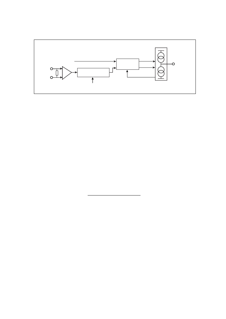
Fig. 23 Auxiliary Synthesiser
The phase detector drives switched current sources to
pump charge onto an external passive loop filter which is
primarily an integrator, resulting in the minimum of external
components. The charge pump output current level is set by
the external resistor on pin RSMA and the ratio is fixed so that
nominal I
= 8 x I
. This bias resistor also sets the main
synthesiser output current but that current has a programm-
able ratio to enable different currents for each loop. The pin
RSMA does not need any decoupling and to avoid all possi-
bilities of oscillation the external capacitance should be less
than 5 pF.
The polarity of the output is such that a more positive
voltage on the loop filter (PDA pin) sets a higher VCO
frequency.
A standby mode for the auxiliary synthesiser can be
selected if bit DA in Word D is HIGH.
This synthesiser is used to add modulation to the trans-
mitted signal. The most convenient approach, as shown in
figure 31, is to drive the positive end of the varactor diode in
the tank circuit with the loop filter to set the frequency and then
to drive the negative end with the modulation from a summing
circuit (speech plus SAT plus data or ST) from ACE9040.
Auxiliary Synthesiser
The Auxiliary Synthesiser operates with an input fre-
quency up to 135 MHz. The input buffer will amplify and limit
a small amplitude sinewave signal and so can be driven from
the ACE9020 VCO directly. There are three main blocks in this
synthesiser: a 12-bit programm-able divider, a digital phase
detector, and output charge pumps to drive a passive loop
filter.
To assist fast recovery from power-down the inputs FIA
and FIAB are designed to be d.c. driven by the TXOSC+ and
TXOSC– outputs from ACE9020.
FIA can also be used single-ended if it is driven by a signal
with double amplitude, the correct d.c. level and if FIAB is
decoupled to ground by a capacitor (see Electrical Character-
istics for full details). Internal biasing will set the d.c. level on
FIAB.
The 12 bit programmable divider is set by the NA bits in
Word C and ratios from 3 to 4095 can be used. This drives the
phase detector along with the comparison frequency signal
from the common reference divider.
A digital phase detector is used and is designed to
eliminate any deadband around the locked state, this is
especially important when modulation is added.
Main Synthesiser
The main synthesiser in the ACE9030 is designed to
operate with a two-modulus prescaler and will accept frequen-
cies up to 30 MHz. To assist fast recovery from power-down
the inputs FIM and FIMB are designed to be d.c. driven by the
DIV_OUT+ and DIV_OUT– outputs from the ACE9020 or
similar outputs from standard prescalers.
FIM can also be used single-ended if it is driven by a signal
with double amplitude, the correct d.c. level and if FIMB is
decoupled to ground by a capacitor (see Electrical Character-
istics for full details). Internal biasing will set the d.c. level on
FIMB.
The block diagram depends on which mode is selected
but is basically the same as the Auxiliary synthesiser with
added features for each mode. The common element is the
phase detector, which is the same circuit used in the Auxiliary
synthesiser and again drives switched current sources to
pump charge into an external passive loop filter to minimise
the external components. The charge pump output current
level is set by the external resistor on pin RSMA and the
multiplying ratio is programmable by the bus and the chosen
mode as in table 6. This bias resistor also sets the Auxiliary
synthesiser output current as described above.
A standby mode for the main synthesiser can be selected
if bit DM in Word D is HIGH.
The Main synthesiser can be used in different modes
depending on the requirements of the communication system
it is operating in:
Normal mode
The most straightforward to use and adequate for most
analogue cellular telephone systems.
Normal Mode with Speed-up
This adds a fast slew drive to the loop filter during channel
changes so that the time from channel to channel is signifi-
cantly reduced but once the change is expected to be com-
plete the loop reverts to normal mode. A little care is needed
in parameter choice and loop filter design to ensure the loop
is stable in both modes and there is likely to be a higher level
of comparison sidebands during speed-up mode. This combi-
nation offers a faster channel change or a lower level of
comparison frequency sidebands once on channel, or with
care some of each advantage.
NA FROM BUS
PHASE
DETECTOR
DOWN
UP
φ
φ
12 BIT DIVIDER
RESET
CHARGE
PUMP
PDA
AUXILIARY COMPARISON
FREQUENCY (FROM
REFERENCE DIVIDER)
FIA
FIAB
相關(guān)PDF資料 |
PDF描述 |
|---|---|
| ACE9030 | Radio Interface and Twin Synthesiser |
| ACE9040 | Audio Processor Advance Information |
| ACE9050 | System Controller and Data Modem(為蜂窩式手機提供控制和邏輯接口功能的系統(tǒng)控制器和數(shù)據(jù)調(diào)制解調(diào)器) |
| ACE9050 | System Controller and Data Modem Advance Information |
| ACFA-450 | AM CERAMIC FILTERS |
相關(guān)代理商/技術(shù)參數(shù) |
參數(shù)描述 |
|---|---|
| ACE9030IGFP1N | 制造商:未知廠家 制造商全稱:未知廠家 功能描述:Parallel-Input Frequency Synthesizer |
| ACE9030IGFP1R | 制造商:未知廠家 制造商全稱:未知廠家 功能描述:Parallel-Input Frequency Synthesizer |
| ACE9030IGFP2N | 制造商:未知廠家 制造商全稱:未知廠家 功能描述:Parallel-Input Frequency Synthesizer |
| ACE9030IGFP2R | 制造商:未知廠家 制造商全稱:未知廠家 功能描述:Parallel-Input Frequency Synthesizer |
| ACE9030M | 制造商:MITEL 制造商全稱:Mitel Networks Corporation 功能描述:Radio Interface and Twin Synthesiser |
發(fā)布緊急采購,3分鐘左右您將得到回復(fù)。