- 您現(xiàn)在的位置:買賣IC網(wǎng) > PDF目錄166215 > AM29LV001BB-70ED (SPANSION LLC) Flash Memory IC; Memory Size:1Mbit; Package/Case:48-TSOP; Supply Voltage Max:3V; Leaded Process Compatible:Yes; Peak Reflow Compatible (260 C):Yes; Access Time, Tacc:70nS; Series:AM29 RoHS Compliant: Yes PDF資料下載
參數(shù)資料
| 型號: | AM29LV001BB-70ED |
| 廠商: | SPANSION LLC |
| 元件分類: | PROM |
| 英文描述: | Flash Memory IC; Memory Size:1Mbit; Package/Case:48-TSOP; Supply Voltage Max:3V; Leaded Process Compatible:Yes; Peak Reflow Compatible (260 C):Yes; Access Time, Tacc:70nS; Series:AM29 RoHS Compliant: Yes |
| 中文描述: | 128K X 8 FLASH 3V PROM, 70 ns, PDSO32 |
| 封裝: | LEAD FREE, MO-142BBD, TSOP-32 |
| 文件頁數(shù): | 43/43頁 |
| 文件大小: | 841K |
| 代理商: | AM29LV001BB-70ED |
第1頁第2頁第3頁第4頁第5頁第6頁第7頁第8頁第9頁第10頁第11頁第12頁第13頁第14頁第15頁第16頁第17頁第18頁第19頁第20頁第21頁第22頁第23頁第24頁第25頁第26頁第27頁第28頁第29頁第30頁第31頁第32頁第33頁第34頁第35頁第36頁第37頁第38頁第39頁第40頁第41頁第42頁當前第43頁
May 5, 2006 21557F4
Am29LV001B
7
DATA SHEE T
DEVICE BUS OPERATIONS
This section describes the requirements and use of the
device bus operations, which are initiated through the
internal command register. The command register
itself does not occupy any addressable memory loca-
tion. The register is composed of latches that store the
commands, along with the address and data informa-
tion needed to execute the command. The contents of
the register serve as inputs to the internal state
machine. The state machine outputs dictate the func-
tion of the device. Table 1 lists the device bus
operations, the inputs and control levels they require,
and the resulting output. The following subsections
describe each of these operations in further detail.
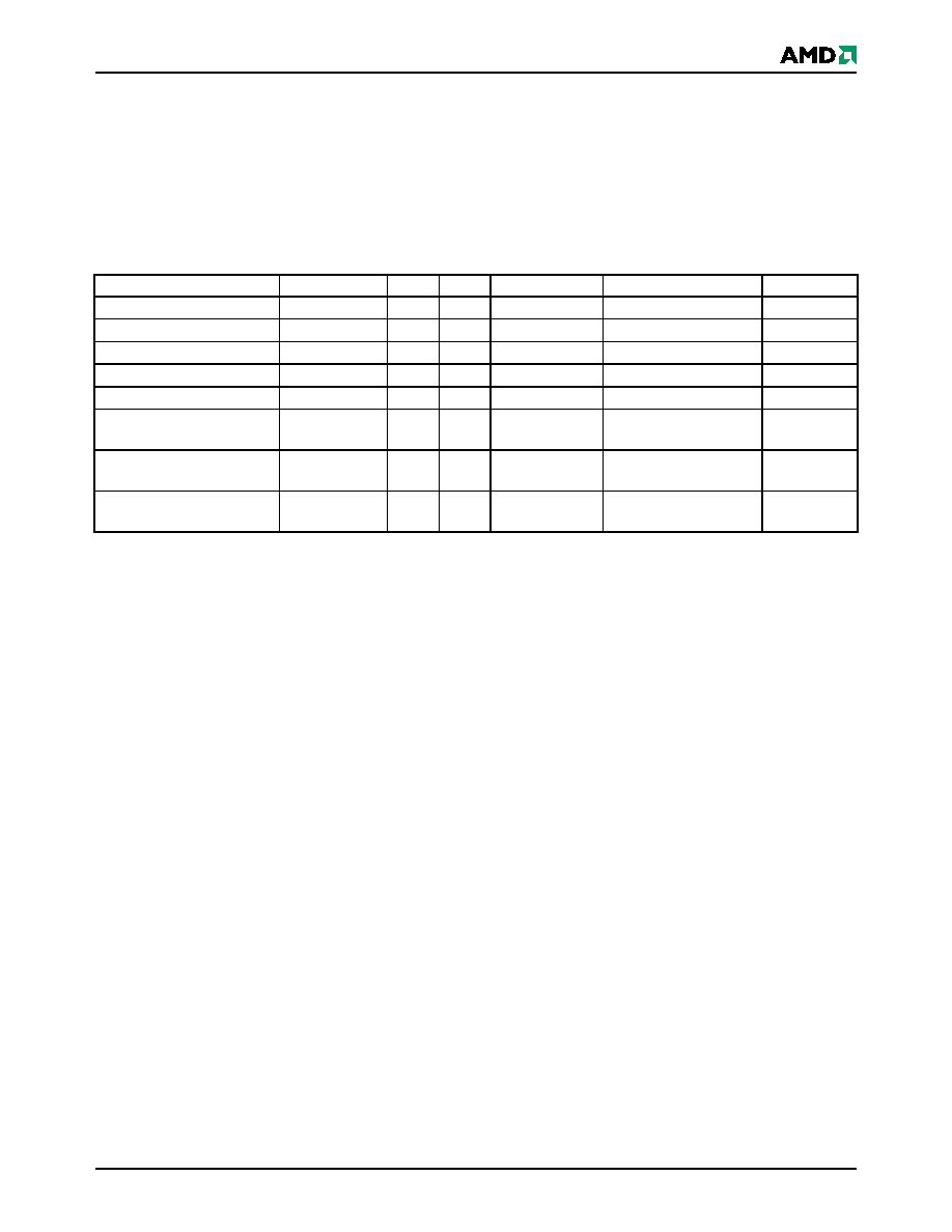
Table 1.
Am29LV001B Device Bus Operations
Legend:
L = Logic Low = VIL, H = Logic High = VIH, VID = 12.0 ± 0.5 V, X = Don’t Care, AIN = Address In, DIN = Data In, DOUT = Data Out
Notes:
1. Addresses are A16–A0.
2. The in-system method of sector protection/unprotection is available. Sector protection/unprotection can be implemented by
using programming equipment. See ““Sector Protection/Unprotection” on page 10” .
Requirements for Reading Array Data
To read array data from the outputs, the system must
drive the CE# and OE# pins to VIL. CE# is the power
control and selects the device. OE# is the output
control and gates array data to the output pins. WE#
should remain at VIH.
The internal state machine is set for reading array data
upon device power-up, or after a hardware reset. This
ensures that no spurious alteration of the memory
content occurs during the power transition. No
command is necessary in this mode to obtain array
data. Standard microprocessor read cycles that assert
valid addresses on the device address inputs produce
valid data on the device data outputs. The device
remains enabled for read access until the command
register contents are altered.
See “Reading Array Data” on page 13 for more infor-
mation. Refer to the AC “Read Operations” on page 26
table for timing specifications and to Figure 13, on page
tics table represents the active current specification for
reading array data.
Writing Commands/Command Sequences
To write a command or command sequence (which
includes programming data to the device and erasing
sectors of memory), the system must drive WE# and
CE# to VIL, and OE# to VIH.
The device features an Unlock Bypass mode to facili-
tate faster programming. Once the device enters the
Unlock Bypass mode, only two write cycles are
required to program a byte, instead of four. The “Byte
contains details on programming data to the device
using both standard and Unlock Bypass command
sequences.
An erase operation can erase one sector, multiple sec-
tors, or the entire device. Table 2 on page 9 indicate the
address space that each sector occupies. A “sector
address” consists of the address bits required to
uniquely select a sector. The “Command Definitions”
on page 13 section contains details on erasing a sector
or the entire chip, or suspending/resuming the erase
operation.
After the system writes the autoselect command
sequence, the device enters the autoselect mode. The
system can then read autoselect codes from the
Operation
CE#
OE#
WE#
RESET#
Addresses (Note 1)
DQ0–DQ7
Read
L
H
AIN
DOUT
Write
L
H
L
H
AIN
DIN
Standby
VCC ± 0.3 V
X
VCC ± 0.3 V
X
High-Z
Output Disable
L
H
X
High-Z
Reset
X
L
X
High-Z
Sector Protect (Note 2)
L
H
L
VID
Sector Address, A6 =
L, A1 = H, A0 = L
DIN, DOUT
Sector Unprotect (Note 2)
L
H
L
VID
Sector Address, A6 =
H, A1 = H, A0 = L
DIN, DOUT
Temporary Sector
Unprotect
XX
X
VID
AIN
DIN
相關PDF資料 |
PDF描述 |
|---|---|
| AM29LV002BB-120ED | Flash Memory IC; Leaded Process Compatible:Yes; Memory Size:2Mbit; Package/Case:48-TSOP; Peak Reflow Compatible (260 C):Yes; Supply Voltage Max:3V; Access Time, Tacc:120ns; Series:AM29 RoHS Compliant: Yes |
| AM29LV002BT-70EF | Flash Memory IC; Leaded Process Compatible:Yes; Memory Size:2Mbit; Package/Case:48-TSOP; Peak Reflow Compatible (260 C):Yes; Supply Voltage Max:3V; Access Time, Tacc:70ns; Series:AM29 RoHS Compliant: Yes |
| AM29LV002BT-90ED | Flash Memory IC; Leaded Process Compatible:Yes; Memory Size:2Mbit; Package/Case:48-TSOP; Peak Reflow Compatible (260 C):Yes; Supply Voltage Max:3V; Access Time, Tacc:90ns; Series:AM29 RoHS Compliant: Yes |
| AM29LV002BT-90EF | Flash Memory IC; Leaded Process Compatible:Yes; Memory Size:2Mbit; Package/Case:48-TSOP; Peak Reflow Compatible (260 C):Yes; Supply Voltage Max:3V; Access Time, Tacc:90ns; Series:AM29 RoHS Compliant: Yes |
| AM29LV004BB-120ED | Flash Memory IC; Leaded Process Compatible:Yes; Memory Size:4Mbit; Package/Case:48-TSOP; Peak Reflow Compatible (260 C):Yes; Supply Voltage Max:3V; Access Time, Tacc:120ns; Series:AM29 RoHS Compliant: Yes |
相關代理商/技術參數(shù) |
參數(shù)描述 |
|---|---|
| AM29LV001BB-90JD | 制造商:Spansion 功能描述:FLASH PARALLEL 3V/3.3V 1MBIT 128KX8 90NS 32PLCC - Rail/Tube |
| AM29LV001BT-55ED | 制造商:Spansion 功能描述:1M (128KX8) 3V, BOOT BLOCK, TOP, TSOP32, COM - Trays |
| AM29LV002BB-90EC | 制造商:Advanced Micro Devices 功能描述: |
| AM29LV002BT-90EF | 制造商:Spansion 功能描述:NOR Flash Parallel 3V/3.3V 2Mbit 256K x 8bit 90ns 40-Pin TSOP |
| AM29LV002BT-90EI\\T | 制造商:Spansion 功能描述:FLASH PARALLEL 3V/3.3V 2MBIT 256KX8 90NS 40TSOP - Tape and Reel |
發(fā)布緊急采購,3分鐘左右您將得到回復。