- 您現(xiàn)在的位置:買賣IC網(wǎng) > PDF目錄362278 > AM486DX Am486DX - Am486DX Block Diagram PDF資料下載
參數(shù)資料
| 型號: | AM486DX |
| 英文描述: | Am486DX - Am486DX Block Diagram |
| 中文描述: | Am486DX - Am486DX框圖 |
| 文件頁數(shù): | 25/52頁 |
| 文件大小: | 1242K |
| 代理商: | AM486DX |
第1頁第2頁第3頁第4頁第5頁第6頁第7頁第8頁第9頁第10頁第11頁第12頁第13頁第14頁第15頁第16頁第17頁第18頁第19頁第20頁第21頁第22頁第23頁第24頁當前第25頁第26頁第27頁第28頁第29頁第30頁第31頁第32頁第33頁第34頁第35頁第36頁第37頁第38頁第39頁第40頁第41頁第42頁第43頁第44頁第45頁第46頁第47頁第48頁第49頁第50頁第51頁第52頁
Am486DE2 Microprocessor
25
SMRAM State Save Map
When SMI is recognized on an instruction boundary, the
CPU core first sets the SMIACT signal Low, indicating to
the system logic that accesses are now being made to
the system-defined SMRAM areas. The CPU then
writes its state to the state save area in the SMRAM.
The state save area starts at SMBASE + [8000h +
7FFFh]. The default CS Base is 30000h; therefore, the
default state save area is at 3FFFFh. In this case, the
CS Base is also referred to as the SMBASE.
If the SMBASE relocation feature is enabled, the
SMRAM addresses can change. The following formula
is used to determine the relocated addresses where the
context is saved: SMBASE + [8000h + Register Offset],
where the default initial SMBASE is 30000h and the
Register Offset is listed in Table 3. Reserved spaces are
for new registers in future CPUs. Some registers in the
SMRAM state save area may be read and changed by
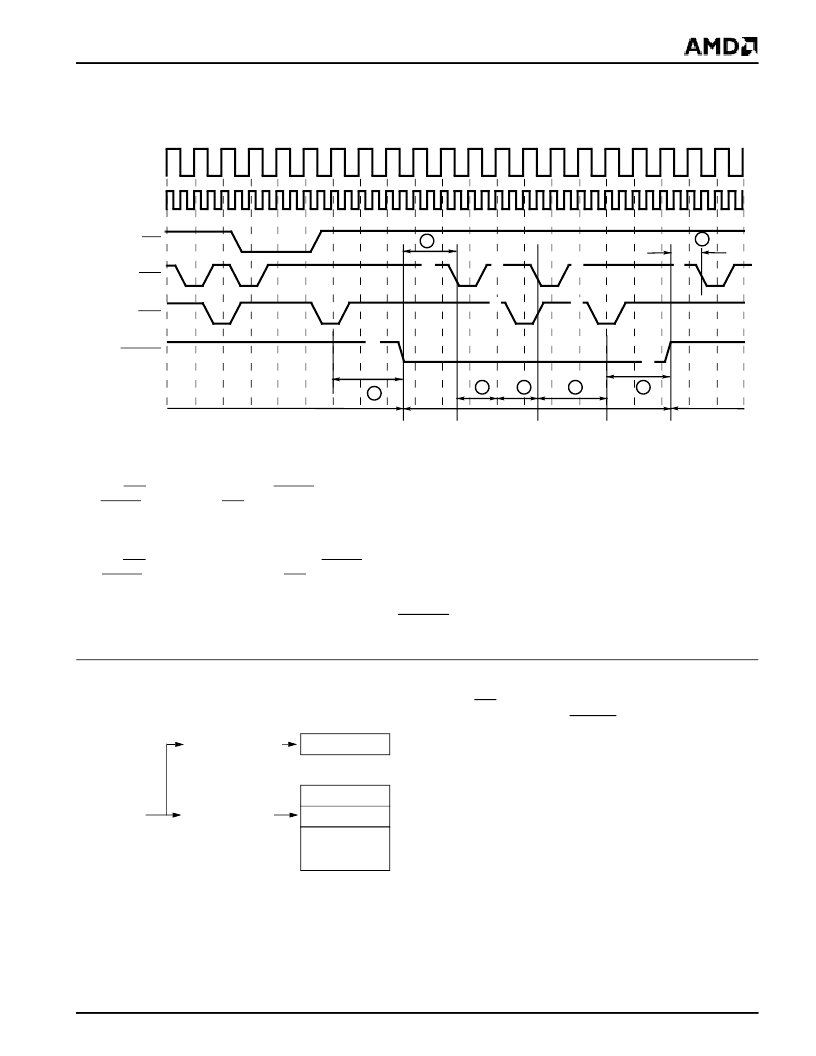
Figure 7. SMIACT Timing
CLK
CLK2
SMI
SMIACT
ADS
RDY
T1
T2
Normal State
State
Save
SMM
Handler
State
Restore
Normal
State
E
Clock-Doubled CPU
2 CLKs minimum
20 CLKs minimum
139 CLKs
User-determined
236 CLKs
2 CLKs minimum
20 CLKs minimum
A: Last RDY from non-SMM transfer to SMIACT assertion
B: SMIACT assertion to first ADS for SMM state save
C: SMM state save (dependent on memory performance)
D: SMI handler
E: SMM state restore (dependent on memory performance)
F: Last RDY from SMM transfer to deassertion of SMIACT
G: SMIACT deassertion of first non-SMM ADS
S S
S S
SS
SS
SS
SS
S S
SS
D
C
A
B
G
F
Figure 8. Redirecting System Memory
Address to SMRAM
SMRAM
System memory
accesses redirected
to SMRAM
System memory
accesses not
redirected to SMRAM
CPU
accesses to
system
address
space used
for loading
SMRAM
Normal
Memory
Space
相關PDF資料 |
PDF描述 |
|---|---|
| AM486DXPGA | Am486DX PGA - Am486DX PGA Package Temperature Comparisons |
| AM486DXSQFP | 70NS, PLCC, IND TEMP(EEPROM) |
| AM486 | Am486 Microprocessor Software User's Manual? 4.40MB (PDF) |
| AM49DL3208G | Am49DL3208G - Stacked Multi-Chip Package (MCP) Flash Memory and pSRAM |
| AM49DL320BG | Am49DL320BG - Stacked Multi-Chip Package (MCP) Flash Memory and SRAM |
相關代理商/技術(shù)參數(shù) |
參數(shù)描述 |
|---|---|
| AM486DX/DX2 | 制造商:未知廠家 制造商全稱:未知廠家 功能描述:Am486DX/DX2 Hardware Reference Manual |
| AM486DX2 | 制造商:AMD 制造商全稱:Advanced Micro Devices 功能描述:Am5X86⑩ Microprocessor Family |
| AM486DX2-66V16BGC | 制造商:Advanced Micro Devices 功能描述:MPU AM486 RISC 32-Bit 0.35um 66MHz 5V 168-Pin PGA |
| AM486DX2-66V16BGI | 制造商:Advanced Micro Devices 功能描述:MPU AM486 RISC 32-Bit 0.35um 66MHz 5V 168-Pin PGA |
| AM486DX2-66V16BHI | 制造商:Advanced Micro Devices 功能描述:MPU AM486 RISC 32-Bit 0.35um 66MHz 5V 208-Pin SQFP |
發(fā)布緊急采購,3分鐘左右您將得到回復。